TRF7960 TRF7961 SLOU186F – AUGUST 2006 – REVISED AUGUST 2010 www.ti.com MULTI-STANDARD FULLY INTEGRATED 13.56-MHZ RFID ANALOG FRONT END AND DATA-FRAMING READER SYSTEM Check for Samples: TRF7960, TRF7961 1 Introduction 1.
TRF7960 TRF7961 SLOU186F – AUGUST 2006 – REVISED AUGUST 2010 www.ti.com Table 1-1. PRODUCT SELECTION TABLE PROTOCOLS DEVICE TRF7960 ISO14443A/B 106 kbps 212 kbps 424 kbps 848 kbps ISO15693 ISO18000-3 Tag-it™ √ √ √ √ √ √ √ √ TRF7961 2 Introduction Copyright © 2006–2010, Texas Instruments Incorporated Submit Documentation Feedback focus.ti.
TRF7960 TRF7961 SLOU186F – AUGUST 2006 – REVISED AUGUST 2010 www.ti.com 1 2 3 4 .............................................. 1.1 Features .............................................. 1.2 APPLICATIONS ...................................... 1.3 Description ........................................... Description (continued) ................................ Physical Characteristics ............................... 3.1 Terminal Functions ................................... 3.
TRF7960 TRF7961 SLOU186F – AUGUST 2006 – REVISED AUGUST 2010 www.ti.com 2 Description (continued) SYS_CLK VDD_X Z – Matching Tx_Out Circuit TRF796x IRQ Rx_IN1 Rx_IN2 Xtal In VDD DATA_CLK MSP430 3 (SPI) Xtal Out VDD_I/O 8 (Parallel) Xtal 13.56 MHz Figure 2-1. Typical Application A parallel or serial interface can be implemented for communication between the MCU and reader. Transmit and receive functions use internal encoders and decoders with a 12-byte FIFO register.
TRF7960 TRF7961 SLOU186F – AUGUST 2006 – REVISED AUGUST 2010 www.ti.com 3 Physical Characteristics 3.1 Terminal Functions Figure 3-1. TRF796x Pin Assignments (Top View) Table 3-1. Terminal Functions TERMINAL NAME NO. TYPE (1) DESCRIPTION OUT Internal regulated supply (2.7 V – 3.4 V) for analog circuitry 2 SUP External supply input to chip (2.7 V – 5.5 V) 3 OUT Internal regulated supply (2.
TRF7960 TRF7961 SLOU186F – AUGUST 2006 – REVISED AUGUST 2010 www.ti.com Table 3-1. Terminal Functions (continued) TERMINAL NAME NO. TYPE (1) DESCRIPTION I/O pin for parallel communication I/O_5 22 BID Strobe out clock for serial communication Data clock output in direct mode I/O pin for parallel communication I/O_6 23 BID MISO for serial communication (SPI) Serial bit data output in direct mode 1 or sub-carrier signal in direct mode 0 I/O pin for parallel communication.
TRF7960 TRF7961 SLOU186F – AUGUST 2006 – REVISED AUGUST 2010 www.ti.com 4 ELECTRICAL SPECIFICATIONS 4.
TRF7960 TRF7961 SLOU186F – AUGUST 2006 – REVISED AUGUST 2010 4.4 www.ti.com ELECTRICAL CHARACTERISTICS over temperature range VS = 5 V (unless otherwise noted) TYP PARAMETER CONDITIONS 25°C –40°C TO 110°C UNIT MIN/ MAX Supply current in power-down mode All systems disabled, including supply-voltage regulators 1 10 μA MAX IPD2 Supply current in power-down mode 2 The reference voltage generator and the VDD_X remain active to support external circuitry.
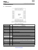
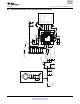
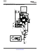
Test Port or Ext Ant Port 0 Ohms 0 Ohms VSWR Adj 27 pF 100 pF Phase Adj open / short / load R “cal” Ant “Q” Adj 680 pF 220 pF VSWR Adj 680 pF 330 nH 10 pF Freq Adj 1000 pF 1000 pF 150 nH Harmonic Suppression 1500 pF 1500 pF 10 nF 2.2 uF 10 nF 2.2 uF 10 nF 2.2 uF 8 7 6 5 4 3 2 1 RX1_AM VSS_RX VSS_RF TX_OUT VDD_PA VDD_RF VIN VDD_A 27 pF 27 pF 30 29 28 27 10 2.2 uF 11 12 14 1K 13 RHB - 32 TRF796x 16 25 1K 15 33 26 10K Thermal Pad 31 13.
Test Port or Ext Ant Port R “cal” 27 pF 100 pF Phase Adj VSWR Adj 0 Ohms 0 Ohms open / short / load 680 pF 220 pF 1000 pF 1000 pF 150 nH Freq Adj Harmonic Suppression VSWR Adj 680 pF 330 nH 10 pF 10 nF 10 nF 1500 pF 1500 pF 10 nF 2.2 µF 8 7 6 5 4 3 2 1 RX1_AM VSS_RX VSS_RF TX_OUT VDD_PA VDD_RF VIN VDD_A 30 29 28 27 10 K 10 11 2.2 µF 12 14 1K 13 RHB - 32 TRF796x Thermal Pad 31 10 nF 9 32 27 pF OSC_IN VSS 2.
TRF7960 TRF7961 SLOU186F – AUGUST 2006 – REVISED AUGUST 2010 www.ti.com 5 System Description 5.1 Power Supplies The positive supply pin, VIN (pin 2) has an input voltage range of 2.7 V to 5.5 V. The positive supply input sources three internal regulators with output voltages VDD_RF, VDD_A and VDD_X that use external bypass capacitors for supply noise filtering. These regulators provide enhanced PSRR for the RFID reader system.
TRF7960 TRF7961 SLOU186F – AUGUST 2006 – REVISED AUGUST 2010 5.1.3 www.ti.com Supply Regulator Configuration The supply regulators can be automatically or manually configured by the control bits. The available options are shown in Table 5-1 through Table 5-4. Table 5-1 shows a 5-V system and the manual-mode regulator settings. Table 5-2 shows manual mode for selection of a 3-V system. Table 5-3 and Table 5-4 show the automatic-mode gain settings for 5-V and 3-V systems.
TRF7960 TRF7961 SLOU186F – AUGUST 2006 – REVISED AUGUST 2010 www.ti.com Table 5-3. Supply-Regulator Setting – Automatic – 5-V System Byte Address Option Bits Setting in Control Register B7 B6 B5 B4 B3 B2 (1) B1 00 (1) Action B0 1 5-V system 0B 1 x 1 1 Automatic regulator setting ≉ 250-mV difference 0B 1 x 1 0 Automatic regulator setting ≉ 350-mV difference 0B 1 x 0 0 Automatic regulator setting ≉ 400-mV difference X are don't cares Table 5-4.
TRF7960 TRF7961 SLOU186F – AUGUST 2006 – REVISED AUGUST 2010 www.ti.com After the reader EN line is high, the other power modes are selected by control bits. The power mode options and functions are listed in Table 5-5. Table 5-5.
TRF7960 TRF7961 SLOU186F – AUGUST 2006 – REVISED AUGUST 2010 www.ti.com 5.1.5 Timing Diagrams CHIP POWER UP TO CLOCK START C001 Figure 5-1. Power Up [VIN (Blue) to Crystal Start (Red)] CHIP ENABLE TO CLOCK START C002 Figure 5-2. EN2 Low and EN High (Blue) to Start of System Clock (Red) System Description Copyright © 2006–2010, Texas Instruments Incorporated Submit Documentation Feedback focus.ti.
TRF7960 TRF7961 SLOU186F – AUGUST 2006 – REVISED AUGUST 2010 www.ti.com CHIP ENABLE TO CLOCK START C003 Figure 5-3. EN2 High and EN Low (Blue) to Start of System Clock (Red) 16 System Description Copyright © 2006–2010, Texas Instruments Incorporated Submit Documentation Feedback focus.ti.
TRF7960 TRF7961 SLOU186F – AUGUST 2006 – REVISED AUGUST 2010 www.ti.com 5.2 Receiver – Analog Section The TRF7960/61 has two receiver inputs, RX_IN1 (pin 8) and RX_IN2 (pin 9). The two inputs are connected to an external filter to ensure that AM modulation from the tag is available on at least one of the two inputs. The external filter provides a 45° phase shift for the RX_IN2 input to allow further processing of a received PM-modulated signal (if it appears) from the tag.
TRF7960 TRF7961 SLOU186F – AUGUST 2006 – REVISED AUGUST 2010 www.ti.com Correlation between the RF input level and RSSI designation levels on the RX_IN1 and RX_IN2 are shown in Table 5-6 and Table 5-7. Table 5-6 shows the RSSI level versus RSSI bit value. The RSSI has seven levels (3 bits each) with 4-dB increments. The input level is the peak-to-peak modulation level of the RF signal as measured on one side envelope (positive or negative). Table 5-6.
TRF7960 TRF7961 SLOU186F – AUGUST 2006 – REVISED AUGUST 2010 www.ti.com The main register controlling the digital part of the receiver is the ISO control register (address 01). By writing to this register, the user selects the protocol to be used. With each new write in this register, the default presets are loaded in all related registers, so no further adjustments in other registers are needed for proper operation. Table 5-10 shows the coding of the ISO control register.
TRF7960 TRF7961 SLOU186F – AUGUST 2006 – REVISED AUGUST 2010 www.ti.com NOTE The crystal oscillator’s two external shunt capacitor values are calculated based crystal’s specified load capacitance. The external capacitors (connected to the OSC and 31), are calculated as two capacitors in series plus CS (oscillator's gate input/output capacitance plus PCB stray capacitance). The stray capacitance (CS) estimated at approximately 5 ±2 pF (typical).
TRF7960 TRF7961 SLOU186F – AUGUST 2006 – REVISED AUGUST 2010 www.ti.com At the end of the transmit operation, the external system is notified by another interrupt request with a flag in the IRQ register that signals the end of TX. The TX length register also supports incomplete bytes transmitted. The high two nibbles in register 1D and the nibble composed of bits B4–B7 in register 1E store the number of complete bytes to be transmitted.
TRF7960 TRF7961 SLOU186F – AUGUST 2006 – REVISED AUGUST 2010 5.2.4 www.ti.com Direct Mode Direct mode allows the user to configure the reader in one of two ways. Direct mode 0 (bit 6 = 0, as defined in ISO control register) allows the user to use only the front-end functions of the reader, bypassing the protocol implementation in the reader. For transmit functions, the user has direct access to the transmit modulator through the MOD pin (pin 14).
TRF7960 TRF7961 SLOU186F – AUGUST 2006 – REVISED AUGUST 2010 www.ti.com Analog Front End (AFE) Mode 0: Raw, Sub-Carrier Data ISO Encoder/Decoders 14443A 14443B 15693 Tag-it Mode 1: Un-Framed Raw ISO Formatted Data Packetization/Framing Mode 2: Full ISO With Framing and Error Checking (Typical Mode) Figure 5-4. User-Configurable Modes 5.2.5 Register Preset After power-up and the EN pin low-to-high transition, the reader is in the default mode.
TRF7960 TRF7961 SLOU186F – AUGUST 2006 – REVISED AUGUST 2010 5.3 www.ti.com Register Descriptions Table 5-8.
TRF7960 TRF7961 SLOU186F – AUGUST 2006 – REVISED AUGUST 2010 www.ti.com 5.3.1 Control Registers – Main Configuration Registers Table 5-9. Chip Status Control (00h) Controls the power mode, RF on / off, AGC, AM / PM Register default is 0x01.
TRF7960 TRF7961 SLOU186F – AUGUST 2006 – REVISED AUGUST 2010 www.ti.com Table 5-10. ISO Control (01h) Controls the ISO selection Register default is 0x02, which is ISO15693 high bit rate, one sub-carrier, 1 out of 4. It is preset at EN = L or POR = H. Bit Bit Name Function Comments B7 rx_crc_n Receiving without CRC 1 = no RX CRC 0 = RX CRC B6 dir_mode Direct mode type 0 = output is sub-carrier data.
TRF7960 TRF7961 SLOU186F – AUGUST 2006 – REVISED AUGUST 2010 www.ti.com 5.3.2 Control Registers – Sub Level Configuration Registers Table 5-12. ISO14443B TX Options (02h) Selects the ISO subsets for ISO14443B – TX Register default is set to 0x00 at POR = H or EN = L Bit Bit Name Function Comments B7 egt2 TX EGT time select MSB B6 egt1 TX EGT time select Three bit code defines the number of etu (0-7) which separate two characters.
TRF7960 TRF7961 SLOU186F – AUGUST 2006 – REVISED AUGUST 2010 www.ti.com Table 5-15. TX Timer L-Byte (05h) Register default is set to 0x00 at POR = H or EN = L and at each write to ISO control register Bit Bit Name Function Comments B7 Tm_length7 Timer length MSB B6 Tm_length6 Timer length B5 Tm_length5 Timer length B4 Tm_length4 Timer length Defines the time when delayed transmission is started. RX wait range is 590 ns to 9.76 ms (1..
TRF7960 TRF7961 SLOU186F – AUGUST 2006 – REVISED AUGUST 2010 www.ti.com Table 5-18. RX Wait Time (08h) Defines the time after TX EOF when the RX input is disregarded Register default is set to 0x1F at POR = H or EN = L and at each write to ISO control register. Bit Bit Name Function Comments B7 Rxw7 RX wait B6 Rxw6 B5 Rxw5 B4 Rxw4 B3 Rxw3 Defines the time during which the RX input is ignored. It starts from the end of TX EOF. RX wait range is 9.44 μs to 2407 μs (1...255), Step size 9.
TRF7960 TRF7961 SLOU186F – AUGUST 2006 – REVISED AUGUST 2010 www.ti.com Table 5-20. RX Special Setting Register (Address 0Ah) Sets the gains and filters directly Register default is set to 0x40 at POR = H or EN = L, and at each write to the ISO control register.
TRF7960 TRF7961 SLOU186F – AUGUST 2006 – REVISED AUGUST 2010 www.ti.com 5.3.3 Status Registers Table 5-22. IRQ Status Register (0Ch) Displays the cause of IRQ and TX/RX status Register default is set to 0x00 at POR = H or EN = L, and at each write to the ISO control register. It is also automatically reset at the end of a read phase. The reset also removes the IRQ flag. Bit Bit Name Function Comments B7 Irq_tx IRQ set due to end of TX Signals that TX is in progress.
TRF7960 TRF7961 SLOU186F – AUGUST 2006 – REVISED AUGUST 2010 www.ti.com Table 5-25. RSSI Levels and Oscillator Status Register (0Fh) Displays the signal strength on both reception channels and RF amplitude during RF-off state The RSSI values are valid from reception start till start of next transmission.
TRF7960 TRF7961 SLOU186F – AUGUST 2006 – REVISED AUGUST 2010 www.ti.com 5.3.4 FIFO Control Registers Table 5-26.
TRF7960 TRF7961 SLOU186F – AUGUST 2006 – REVISED AUGUST 2010 5.4 5.4.1 www.ti.com Direct Commands From MCU to Reader Command Codes Table 5-29.
TRF7960 TRF7961 SLOU186F – AUGUST 2006 – REVISED AUGUST 2010 www.ti.com the RF and receivers are switched ON. When this command is received, the reader observes the digitized receiver output. If more than two edges are observed in 100 μs, the window comparator voltage is increased. The procedure is repeated until the number of edges (changes of logical state) of the digitized reception signal is less than 2 (in 100 μs). The command can reduce the input sensitivity in 5-dB increments up to 15 dB.
TRF7960 TRF7961 SLOU186F – AUGUST 2006 – REVISED AUGUST 2010 5.5 www.ti.com Reader Communication Interface 5.5.1 Introduction The communication interface to the reader can be configured in two ways: a parallel 8-pin interface and a Data_Clk or a serial peripheral interface (SPI). These modes are mutually exclusive; only one mode can be used at a time in the application. When the SPI interface is selected, the unused I/O_2, I/O_1, and I/O_0 pins must be hard-wired according to Table 5-30.
TRF7960 TRF7961 SLOU186F – AUGUST 2006 – REVISED AUGUST 2010 www.ti.com The MSB (bit 7) determines if the word is to be used as a command or as an address. The last two columns of Table 5-31 show the function of the separate bits if either address or command is written. Data is expected once the address word is sent. In continuous-address mode (Cont. mode = 1), the first data that follows the address is written (or read) to (from) the given address.
TRF7960 TRF7961 SLOU186F – AUGUST 2006 – REVISED AUGUST 2010 5.6 www.ti.com Parallel Interface Communication In parallel mode, the start condition is generated on the rising edge of the I/O_7 pin while the CLK is high. This is used to reset the interface logic. Figure 5-5 shows the sequence of the data, with an 8-bit address word first, followed by data.
TRF7960 TRF7961 SLOU186F – AUGUST 2006 – REVISED AUGUST 2010 www.ti.com 5.6.1 Receive At the start of a receive operation (when SOF is successfully detected), B6 is set in the IRQ status register. An interrupt request is sent to the MCU at the end of the receive operation if the receive data string was shorter than or equal to 8 bytes.
TRF7960 TRF7961 SLOU186F – AUGUST 2006 – REVISED AUGUST 2010 5.7 www.ti.com Serial Interface Communication When an SPI interface is required, parallel I/O pins, I/O_2, I/O_1, and I/O_0, must be hard wired according to Table 5-31. On power up, the reader looks for the status of these pins; if they are not the same (not all high, or not all low), the reader enters into one of two possible SPI modes.
TRF7960 TRF7961 SLOU186F – AUGUST 2006 – REVISED AUGUST 2010 www.ti.com Write Operation SCLK MOSI B7 B6 B5 B4 B3 B2 B1 B0 SS* Figure 5-9. Serial–SPI Interface Communication (Write Mode) System Description Copyright © 2006–2010, Texas Instruments Incorporated Submit Documentation Feedback focus.ti.
TRF7960 TRF7961 SLOU186F – AUGUST 2006 – REVISED AUGUST 2010 www.ti.com The SPI read operation is shown in Figure 5-10.
TRF7960 TRF7961 SLOU186F – AUGUST 2006 – REVISED AUGUST 2010 www.ti.com Continuous Read Operation Write Address Byte Read Data Byte 1 Read Data Byte n MOSI B7 B6 B5 B4 B3 B2 B1 B0 No Data Transitions (All High/Low) No Data Transitions (All High/Low) MISO Don’t Care B7 B6 B5 B4 B3 B2 B1 B0 B7 B6 B5 B4 B3 B2 B1 B0 SCLK SS* Figure 5-11. SPI Interface Communication (Continuous Read Mode) Note: Special steps are needed to read the TRF796x IRQ status register (register address 0x0C) in SPI mode.
TRF7960 TRF7961 SLOU186F – AUGUST 2006 – REVISED AUGUST 2010 5.7.2.1 www.ti.com FIFO Operation The FIFO is a 12-byte register at address 1Fh with byte storage locations 0 to 11. FIFO data is loaded in a cyclical manner and can be cleared by a reset command (0F). Associated with the FIFO are two counters and three FIFO status flags. The first counter is a 4-bit FIFO byte counter (bits B0–B3 in register 1Ch) that keeps track of the number of bytes loaded into the FIFO.
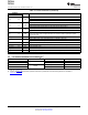
PACKAGE OPTION ADDENDUM www.ti.
PACKAGE MATERIALS INFORMATION www.ti.com 14-Jul-2012 TAPE AND REEL INFORMATION *All dimensions are nominal Device Package Package Pins Type Drawing TRF7960RHBR QFN RHB 32 SPQ Reel Reel A0 Diameter Width (mm) (mm) W1 (mm) B0 (mm) K0 (mm) P1 (mm) W Pin1 (mm) Quadrant 3000 330.0 12.4 5.3 5.3 1.5 8.0 12.0 Q2 TRF7960RHBT QFN RHB 32 250 180.0 12.4 5.3 5.3 1.5 8.0 12.0 Q2 TRF7961RHBR QFN RHB 32 3000 330.0 12.4 5.3 5.3 1.5 8.0 12.
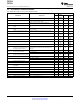
PACKAGE MATERIALS INFORMATION www.ti.com 14-Jul-2012 *All dimensions are nominal Device Package Type Package Drawing Pins SPQ Length (mm) Width (mm) Height (mm) TRF7960RHBR QFN RHB 32 3000 367.0 367.0 35.0 TRF7960RHBT QFN RHB 32 250 210.0 185.0 35.0 TRF7961RHBR QFN RHB 32 3000 367.0 367.0 35.0 TRF7961RHBT QFN RHB 32 250 210.0 185.0 35.
IMPORTANT NOTICE Texas Instruments Incorporated and its subsidiaries (TI) reserve the right to make corrections, enhancements, improvements and other changes to its semiconductor products and services per JESD46, latest issue, and to discontinue any product or service per JESD48, latest issue. Buyers should obtain the latest relevant information before placing orders and should verify that such information is current and complete.