Gleichmann & Co. Electronics GmbH Industriestrasse 16 76297 Stutensee-Spöck / Germany SPECIFICATION CUSTOMER : MODULE NO.: GE-C1604A-TMI-JT/R APPROVED BY: ( FOR CUSTOMER USE ONLY ) PCB VERSION: SALES BY APPROVED BY CHECKED BY DATA: PREPARED BY ISSUED DATE: VERSION DATE A 2008/10/17 GE-C1604A-TMI-JT/R REVISED SUMMARY PAGE NO. 13 page 1 / 26 Modify Character Generator ROM Pattern 11.07.
MODLE NO: DOC. FIRST ISSUE RECORDS OF REVISION VERSION DATE 0 A 2006.10.02 2008/10/17 GE-C1604A-TMI-JT/R REVISED PAGE SUMMARY NO. 13 page 2 / 26 First issue Modify Character Generator ROM Pattern 11.07.
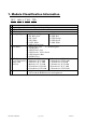
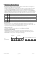
Contents 1. Module Classification Information 2. Precautions in use of LCD Modules 3. General Specification 4. Absolute Maximum Ratings 5. Electrical Characteristics 6. Optical Characteristics 7. Interface Pin Function 8. Contour Drawing & Block Diagram 9. Function Description 10. Character Generator ROM Pattern 11. Instruction Table 12. Timing Characteristics 13. Initializing of LCM 14. Reliability 15. Backlight Information 16. Inspection specification 17.
1. Module Classification Information GE-C 1604 A –T M I- JT/R Brand:Gleichmann Electronics Display Type:C→Character Type, G→Graphic Type Display Font:Character 16 words, 4 lines. Model serials no.
2. Precautions in use of LCD Modules (1)Avoid applying excessive shocks to the module or making any alterations or modifications to it. (2)Don’t make extra holes on the printed circuit board, modify its shape or change the components of LCD module. (3)Don’t disassemble the LCM. (4)Don’t operate it above the absolute maximum rating. (5)Don’t drop, bend or twist LCM. (6)Soldering: only to the I/O terminals. (7)Storage: please storage in anti-static electricity container and clean environment. 3.
4.Absolute Maximum Ratings Item Symbol Min Typ Max Unit Operating Temperature TOP -20 - +70 ℃ Storage Temperature TST -30 - +80 ℃ Input Voltage VI VSS - VDD V Supply Voltage For Logic VDD-VSS -0.3 - 7 V Supply Voltage For LCD VDD-V0 -0.3 - 13 V 5.Electrical Characteristics Item Supply Voltage For Logic Symbol Condition Min Typ Max Unit VDD-VSS - 4.5 5.0 5.5 V Ta=-20℃ - - 5.7 V Ta=25℃ - 4.5 - V Ta=70℃ 3.
6.
7.Interface Pin Function Pin No. Symbol Level Description 1 VSS 0V 2 VDD 5.
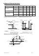
8.Contour Drawing &Block Diagram 2.5 11.3 17 19.6 1 2 3 4 5 6 7 8 9 10 11 12 13 14 15 16 16 1 55.0 60.0 0.5 37.4 26.0(VA) 20.8(AA) 13.6 MAX 9.0 2.5 87.0 0.5 P2.54*15=38.1 2.0 16- 1.0 10.0 2.5 15.4 12.5 82.0 56.2(AA) 62.0(VA) 1.6 4- 2.5 PTH 4- 5.0 PAD LED B/L 79 4 2.95 0.6 Vss Vdd Vo RS R/W E DB0 DB1 DB2 DB3 DB4 DB5 DB6 DB7 A K 0.6 0.55 0.3mm. 0.6 4.75 0.6 0.55 The non-specified tolerance of dimension is DOT SIZE SCALE 5/1 Vdd Vo Vss VR 10K~20K Vee External contrast adjustment.
9.Function Description The LCD display Module is built in a LSI controller, the controller has two 8-bit registers, an instruction register (IR) and a data register (DR). The IR stores instruction codes, such as display clear and cursor shift, and address information for display data RAM (DDRAM) and character generator (CGRAM). The IR can only be written from the MPU. The DR temporarily stores data to be written or read from DDRAM or CGRAM.
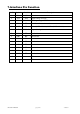
Display position DDRAM address 1 2 3 4 5 6 7 8 9 10 11 12 13 14 15 16 00 40 10 50 01 41 11 51 02 03 04 05 06 07 08 42 43 44 45 46 47 48 12 13 14 15 16 17 18 52 53 54 55 56 57 58 4-Line by 16-Character Display 09 49 19 59 0A 4A 1A 5A 0B 4B 1B 5B 0C 4C 1C 5C 0D 4D 1D 5D 0E 4E 1E 5E 0F 4F 1F 5F Character Generator ROM (CGROM) The CGROM generate 5×8 dot or 5×10 dot character patterns from 8-bit character codes. See Table 2.
Relationship between CGRAM Addresses, Character Codes (DDRAM) and Character patterns Table 1.
10.Character Generator ROM Pattern Table.2 Upper 4 bit Lower 4 bit LLLL LLLH LLHL LLHH LHLL LHLH LHHL LHHH HLLL HLLH HLHL HLHH HHLL HHLH HHHL HHHH LLLL CG RAM (1) LLLH (2) LLHL (3) LLHH (4) LHLL (5) LHLH (6) LHHL (7) LHHH (8) HLLL (1) HLLH (2) HLHL (3) HLHH (4) HHLL (5) HHLH (6) HHHL (7) HHHH (8) GE-C1604A-TMI-JT/R page 13 / 26 11.07.
11.Instruction Table Instruction Code Instruction Execution time Description (fosc=270Khz) RS R/W DB7 DB6 DB5 DB4 DB3 DB2 DB1 DB0 Clear Display 0 0 0 0 0 0 0 0 0 1 Write “00H” to DDRAM and set DDRAM address to “00H” from AC 1.53ms 1.53ms Return Home 0 0 0 0 0 0 0 0 1 - Set DDRAM address to “00H” from AC and return cursor to its original position if shifted. The contents of DDRAM are not changed.
12.Timing Characteristics 12.1 Write Operation Ta=25℃, VDD=5.0V Item Symbol Min Typ Max Unit Enable cycle time TC 1200 - - ns Enable pulse width TPW 140 - - ns Enable rise/fall time TR,TF - - 25 ns Address set-up time (RS, R/W to E) tAS 0 - - ns Address hold time tAH 10 - - ns Data set-up time tDSW 40 - - ns tH 10 - - ns Data hold time GE-C1604A-TMI-JT/R page 15 / 26 11.07.
12.2 Read Operation Ta=25℃, VDD=5V Item Symbol Min Typ Max Unit TC 1200 - - ns TPW 140 - - ns TR,TF - - 25 ns Address set-up time (RS, R/W to E) tAS 0 - - ns Address hold time tAH 10 - - ns Data delay time tDDR - - 100 ns Data hold time tH 10 - - ns Enable cycle time Enable pulse width (high level) Enable rise/fall time GE-C1604A-TMI-JT/R page 16 / 26 11.07.
13.Initializing of LCM Power on Wait for more than 40 ms after VDD rises to 4.5 V BF can not be checked before this instruction. RS R/W DB7 DB6 DB5 DB4 DB3 DB2 DB1 DB0 Function set 0 0 * * * * 0 0 1 1 Wait for more than 39us BF can not be checked before this instruction. RS R/W DB7 DB6 DB5 DB4 DB3 DB2 DB1 DB0 0 0 0 0 1 0 * * * * 0 0 N F * * * * * * Function set Wait for more than 39 µs BF can not be checked before this instruction.
Power on Wait for more than 40 ms after VDD rises to 4.5 V BF can not be checked before this instruction. RS R/WDB7 DB6 DB5 DB4 DB3 DB2 DB1 DB0 Function set 0 0 0 0 1 1 N F * * Wait for more than 39us BF can not be checked before this instruction.
14. Reliability Content of Reliability Test (wide temperature, -20°C~70°C) Environmental Test Test Item High Temperature storage Low Temperature storage High Temperature Operation Low Temperature Operation High Temperature/ Humidity Operation Thermal shock resistance Content of Test Endurance test applying the high storage temperature for a long time. Endurance test applying the high storage temperature for a long time.
15.Backlight Information Specification PARAMETER SYMBOL MIN TYP MAX UNIT TEST Supply Current ILED 43.2 48 75 mA V=3.5V Supply Voltage V 3.4 3.5 3.6 V - Reverse Voltage VR - - 5 V - Luminous Intensity IV 150 - - CD/M2 ILED=48mA Chromaticity ─ 0.300 - X Y CONDITION 0.310 ILED≦ ≦48mA LED Life Time (For Reference only) - Color White - 50K - Hr. 25℃ ℃,50-60%RH, (Note 1) Note: The LED of B/L is drive by current only, drive voltage is for reference only.
16. Inspection specification NO 01 02 Item Criterion AQL Electrical Testing 1.1 Missing vertical, horizontal segment, segment contrast defect. 1.2 Missing character , dot or icon. 1.3 Display malfunction. 1.4 No function or no display. 1.5 Current consumption exceeds product specifications. 1.6 LCD viewing angle defect. 1.7 Mixed product types. 1.8 Contrast defect. 0.65 Black or white 2.1 White and black spots on display ≦0.25mm, no more than spots on LCD three white or black spots present.
NO Item 05 Scratches Criterion AQL Follow NO.3 LCD black spots, white spots, contamination Symbols Define: x: Chip length y: Chip width z: Chip thickness k: Seal width t: Glass thickness a: LCD side length L: Electrode pad length: 6.1 General glass chip : 6.1.1 Chip on panel surface and crack between panels: 06 Chipped glass z: Chip thickness y: Chip width x: Chip length Z≦1/2t Not over viewing area x≦1/8a 1/2t<z≦2t Not exceed 1/3k x≦1/8a 2.
NO Item Criterion AQL Symbols : x: Chip length y: Chip width z: Chip thickness k: Seal width t: Glass thickness a: LCD side length L: Electrode pad length 6.2 Protrusion over terminal : 6.2.1 Chip on electrode pad : y: Chip width x: Chip length z: Chip thickness y≦0.5mm x≦1/8a 0<z≦t 6.2.2 Non-conductive portion: 06 Glass crack 2.
NO Item 07 Cracked glass 08 09 10 Backlight elements Bezel PCB、COB Criterion AQL The LCD with extensive crack is not acceptable. 2.5 8.1 Illumination source flickers when lit. 8.2 Spots or scratched that appear when lit must be judged. Using LCD spot, lines and contamination standards. 8.3 Backlight doesn’t light or colour wrong. 0.65 2.5 0.65 9.1 Bezel may not have rust, be deformed or have fingerprints, stains or other contamination. 9.2 Bezel must comply with job specifications. 2.5 0.
NO Item Criterion AQL 12.1 No oxidation, contamination, curves or, bends on interface Pin (OLB) of TCP. 12.2 No cracks on interface pin (OLB) of TCP. 12.3 No contamination, solder residue or solder balls on product. 12.4 The IC on the TCP may not be damaged, circuits. 12.5 The uppermost edge of the protective strip on the interface pin must be present or look as if it cause the interface pin to sever. 12 General appearance 12.
17. Material list of components for RoHS 1. The manufacturer hereby declares that all of or part of products (with the mark “/R” in code), including, but not limited to, the LCM, accessories or packages, manufactured and/or delivered to your company (including your subsidiaries and affiliated company) directly or indirectly by our company (including our subsidiaries or affiliated companies) do not intentionally contain any of the substances listed in EU-Directive 2002/95/EC.