Gleichmann & Co. Electronics GmbH Industriestrasse 16 76297 Stutensee-Spöck / Germany SPECIFICATION CUSTOMER : MODULE NO.: GE-O12864D3-TFH/R APPROVED BY: ( FOR CUSTOMER USE ONLY ) PCB VERSION: SALES BY APPROVED BY CHECKED BY DATA: PREPARED BY ISSUED DATE: VERSION DATE 0 2009/8/27 GE-O12864D3-TFH/R REVISED SUMMARY PAGE NO. First issue Page 1/22 21.09.
Contents 1. Module classification information 2. Precautions in Use of LCD Modules 3. General Specification 4. Absolute Maximum Ratings 5. Electrical Characteristics 6. Optical Characteristics 7. Interface Pin Function 8. Counter Drawing and Block Diagram 9. Timing Characteristics 10. Reliability 11.Backlight Information 12. Inspection specification 13. Material List of Components for RoHs GE-O12864D3-TFH/R Page 2/22 21.09.
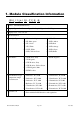
1. Module Classification Information GE-O 1 2 8 6 4 D3 – T F H /R Brand:Gleichmann Electronics Display Type:C→Character Type, G→Graphic Type, O→COG Type Display Font:128 * 64 dots Model serials no.
2. Precautions in Use of LCD Module (1)Avoid applying excessive shocks to the module or making any alterations or modifications to it. (2)Don’t make extra holes on the printed circuit board, modify its shape or change the components of LCD Module. (3)Don’t disassemble the LCM. (4)Don’t operate it above the absolute maximum rating. (5)Don’t drop, bend or twist LCM. (6)Soldering:only to the I/O terminals. (7)Storage:pleasse storage in anti-static electricity container and clean enviroment. 3.
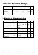
4.Absolute Maximum Ratings Item Symbol Min Typ Max Unit Operating Temperature TOP -20 - +70 ℃ Storage Temperature TST -30 - +80 ℃ Input Voltage VI -0.3 - VDD+0.3 V VDD-VSS -0.3 5.0 V VOUT 4 13 V Supply Voltage For Logic LCD Driver Supply Voltage 5.Electrical Characteristics Item Supply Voltage For Logic Supply Voltage For LCM Symbol Condition Min Typ Max Unit VDD-VSS - 3.0 3.3 3.6 V Ta=-20℃ 10.0 10.2 10.4 V Ta=25℃ 9.8 10.0 10.2 V Ta=70℃ 9.6 9.8 10.
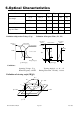
.Optical Characteristics Item Symbol Condition Min Typ Max Unit (V)θ CR≧2 30 - 60 deg (H)φ CR≧2 -45 - 45 deg CR - - 5 - - T rise - - 200 300 ms T fall - - 250 350 ms View Angle Contrast Ratio Response Time Definition of Operation Voltage (Vop) Intensity 100% Definition of Response Time ( Tr , Tf ) Non-selected Conition Selected Wave Non-selected Wave Selected Conition Non-selected Conition Intensity 10% Cr Max Cr = Lon / Loff Vop 90% 100% Tr Driving Voltage
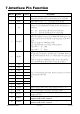
.Interface Pin Function Pin No. Symbol Level Description 1 /CS1 This is the chip select signal. When /CS1 = “L” , then the chip select becomes active, and data/command I/O is enabled. 2 /RES When /RES is set to “L” , the settings are initialized. This is connect to the least significant bit of the normal MPU address bus, and it determines whether the data bits are data or a command. A0 = “H”: Indicates that D0 to D7 are display data. A0 = “L”: Indicates that D0 to D7 are control data.
19 CAP1- 20 CAP1+ 21 CAP2+ 22 CAP2- 23 CAP4+ 24 VRS 25 V4 26 V3 27 V2 28 V1 29 V0 30 VR 31 C86 32 P/S 33 /HPM GE-O12864D3-TFH/R DC/DC voltage converter. Connect a capacitor between this terminal and the CAP1+ terminal. DC/DC voltage converter. Connect a capacitor between this terminal and the CAP1- terminal. DC/DC voltage converter. Connect a capacitor between this terminal and the CAP2- terminal. DC/DC voltage converter.
34 IRS GE-O12864D3-TFH/R This terminal selects the resistors for the V5 voltage level adjustment. IRS = “H”: Use the internal resistors IRS = “L”: Do not use the internal resistors. The V5 voltage level is regulated by an external resistive voltage divider attached to the VR terminal Page 9/22 21.09.
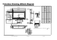
8.Contour Drawing &Block Diagram 80.0¡ Ó 0 .5 7 6.1(LCD) 4.65 7 0.7(VA) 6.74 6 6.52(AA) 9.7¡ Ó 0 .5 6.5 1.7 0.5 3.2 2- 0.6 1.0 1.6 44.2 12.0 D E TA IL B SCALE 2/1 34 4.0¡ Ó 1.0 1.5Max 8.0¡ Ó 1.0 22.25 20.0 3.7 1 0.3 ¡ Ó 0 .05 1.9 (31.25) 1 6.5 68.0 79.
9. Timing Characteristics Reference to Sitronix ST7565P.pdf GE-O12864D3-TFH/R page 11 / 19 13.07.
10. Reliability Content of Reliability Test (wide temperature, -20°C~70°C) Environmental Test Test Item Content of Test Test Condition Note High Temperature storage Endurance test applying the high storage temperature for a long time. 80℃ 200hrs 2 Low Temperature storage Endurance test applying the high storage temperature for a long time.
11.Backlight Information Specification PARAMETER SYMBOL MIN TYP MAX Supply Current ILED Supply Voltage V Reverse Voltage VR - IV 672.8 UNIT TEST 86.4 96 3.4 CONDITION 144 mA V= 3.5 V 3.5 3.6 V - - 5 V - Luminous Intensity 755 - CD/M2 ILED= 96 mA (Without LCD) ILED≦96 mA LED Life Time (For Reference - 50K only) Hr.
12. Inspection specification NO 01 02 Item Criterion AQL Electrical Testing 1.1 Missing vertical, horizontal segment, segment contrast defect. 1.2 Missing character , dot or icon. 1.3 Display malfunction. 1.4 No function or no display. 1.5 Current consumption exceeds product specifications. 1.6 LCD viewing angle defect. 1.7 Mixed product types. 1.8 Contrast defect. 0.65 Black or white 2.1 White and black spots on display ≦0.25mm, no more than spots on LCD three white or black spots present.
NO Item 05 Scratches Criterion AQL Follow NO.3 LCD black spots, white spots, contamination Symbols Define: x: Chip length y: Chip width z: Chip thickness k: Seal width t: Glass thickness a: LCD side length L: Electrode pad length: 6.1 General glass chip : 6.1.1 Chip on panel surface and crack between panels: 06 Chipped glass z: Chip thickness y: Chip width x: Chip length Z≦1/2t Not over viewing area x≦1/8a 1/2t<z≦2t Not exceed 1/3k x≦1/8a 2.
NO Item Criterion AQL Symbols : x: Chip length y: Chip width z: Chip thickness k: Seal width t: Glass thickness a: LCD side length L: Electrode pad length 6.2 Protrusion over terminal : 6.2.1 Chip on electrode pad : y: Chip width x: Chip length z: Chip thickness y≦0.5mm x≦1/8a 0<z≦t 6.2.2 Non-conductive portion: 06 Glass crack 2.
NO Item 07 Cracked glass 08 09 10 Backlight elements Bezel PCB、COB Criterion AQL The LCD with extensive crack is not acceptable. 2.5 8.1 Illumination source flickers when lit. 8.2 Spots or scratched that appear when lit must be judged. Using LCD spot, lines and contamination standards. 8.3 Backlight doesn’t light or colour wrong. 0.65 2.5 0.65 9.1 Bezel may not have rust, be deformed or have fingerprints, stains or other contamination. 9.2 Bezel must comply with job specifications. 2.5 0.
NO Item Criterion AQL 12.1 No oxidation, contamination, curves or, bends on interface Pin (OLB) of TCP. 12.2 No cracks on interface pin (OLB) of TCP. 12.3 No contamination, solder residue or solder balls on product. 12.4 The IC on the TCP may not be damaged, circuits. 12.5 The uppermost edge of the protective strip on the interface pin must be present or look as if it cause the interface pin to sever. 12 General appearance 12.
13. Material list of components for RoHS 1. The manufacturer hereby declares that all of or part of products (with the mark “/R” in code), including, but not limited to, the LCM, accessories or packages, manufactured and/or delivered to your company (including your subsidiaries and affiliated company) directly or indirectly by our company (including our subsidiaries or affiliated companies) do not intentionally contain any of the substances listed in EU-Directive 2002/95/EC.