
User's Manual
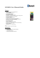

The above schematic shows a typical application ofBC830RPAmodulewith PIOs running at 1.8v.
Power supply
The whole module shall bepowered by a single cell 3.7v Li-ion rechargeable battery(VBAT, pin#34). A coupling
capacitorof 2.2uFshould be placed as close to this pin as possible.The module will output 1.8v at VPAD (pin #28).All
PIO pins, SPI programming port and UART port will runonthis power rail.
Differential Audio Outputs
The output stage digital circuitry converts the signal from 16-bit per sample, linear PCM of variable samplingfrequencyto
bit stream, which is fed into the analogue output circuitry.The output stage circuit comprises a DAC with gain setting and class AB
output stage amplifier. The output isavailable as a differential signal between SPK_LN and SPK_LP for the left channel, asthe
schematicshows,and between SPK_RN and SPK_RP for the right channel.The output stage is capable of driving a speaker directly
when its impedance isat least 8Ω.
UART Port
BC830RPAhas a standard UART serial interface that provides a simple mechanism forcommunicating with other serial
devices using the RS232 protocol.A typical application will beconnecting to an external HCI host.WhenBC830RPAisconnected
to another digital device, RX and TX transfer data between the 2 devices.UART configuration parameters, such as baud rate and
packet format, are setby configuration of theBC8630ROM chip.
To communicate with the UART at its maximum data rate usinga standard PC, an accelerated serial port adaptercard is required for
the PC.
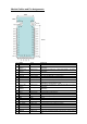
Possible UART Settings
ParameterPossible values
Minimum1200 baud (≤2%Error)Baud rate
Maximum9600 baud (≤1%Error)
ParityNone, Odd or Even
Number of stop bits1 or 2
Bits per byte8
SPI Programming Port
The SPI is used to program and configure the ROM firmware insideBC8630chip.It isrequired in production. Ensure the4
SPI signals are brought out to either test points or a header.Note that these four signalswillrunonthe1.8v power rail.
LED Drivers
BC830RPAincludes 2 pads dedicated to driving LED indicators. Both terminals can be controlledby firmware, The
terminals are open-drain outputs, so the LED must be connected from a positive supply rail to the pad in serieswith a current
limiting resistor.It is recommendedthat the LED pad, LED[0] or LED[1] pins, operate with a pad voltage below 0.5V. In thiscase,
the pad is like a resistor, RON.The resistance together with the external series resistor sets the currentin theLED.
Buttons
The example application has assigned the following functions to each PIO pins:
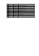
PIN
NAME
FunctionDescriptions
13
PIO17REVSelect previous song, fast rewind.
29PIO18FWDSelect next song, fast forward
14PIO21PLAY_PAUSEPlay / pause toggle
18PIO6VOL-Volumedecrease
15PIO13VOL+Volume increase
39VREGVREG_ENPoweron, sleep mode
Battery and Charging
The whole circuit is running with single cell 3.7v Li-ion battery connecting to the VBAT terminal. VBAT_SENSE is
shorted to this terminal for battery level detection. 5V charging input coming from the micro USB port is connected to the VCHG
terminal. In typicalheadset application, a maximum of 150mA charging current can be supportedwith internal charging.However,
external components can be added to boost the charging current to 500mA if needed.Note that a decoupling capacitor of 2.2uF
should be connected to VCHG.