
Data Sheet
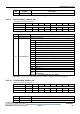
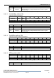

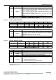
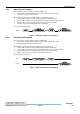
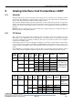
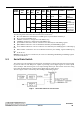
Table Of Contents
- Contents
- Tables
- Figures
- 1 Product Overview
- 2 Functional Description
- 3 FM17520 Register Set
- 4 Host Interfaces
- 5 Analog Interface And Contactless UART
- 6 CRC Coprocessor
- 7 FIFO Buffer
- 8 Interrupt Request System
- 9 Timer
- 10 Power Reduction Modes
- 11 Low Voltage Detection
- 12 Oscillator Circuitry
- 13 Reset And Oscillator Start-Up Time
- 14 Command Set
- 15 Testsignals
- 16 Typical Application Diagram
- 17 Characteristics
- 18 Ordering Information
- 19 Package Information
- Revision History
- Sales and Service

4 Host Interfaces
Datasheet
FM17520 Contactless Transceiver IC Ver 1.0 45
4 Host Interfaces
4.1 SPI Interface
A serial peripheral interface (SPI compatible) is supported by FM17520 to enable high-speed (up to
10Mbit/s) communication to the host. The FM17520 acts as a slave during SPI communication.
The SPI clock signal SCK must be generated by the master. Data bytes on both MOSI and MISO lines are
sent with the MSB first. Data on both MOSI and MISO lines must be stable on the rising edge of the clock
and can be changed on the falling edge.
4.1.1 SPI Read Data
Reading data using SPI requires the byte order shown in Tab 4-1 to be used. The first byte sent
defines both the mode and the address.
Line
Byte 0
Byte 1
Byte 2
To
Byte n
Byte n+1
MOSI
address 0
address 1
address 2
……
address n
00
MISO
X
data 0
data 1
……
data n-1
data n
Tab4-1 MOSI and MISO byte order
4.1.2 SPI Write Data
Writing data using SPI requires the byte order shown in Tab 4-2 to be used. The first byte sent defines
both the mode and the address.
Line
Byte 0
Byte 1
Byte 2
To
Byte n
Byte n+1
MOSI
address 0
data 0
data 1
……
data n-1
data n
MISO
X
X
X
……
X
X
Tab4-2 MOSI and MISO byte order
4.1.3 SPI Address Byte
The first byte, defining mode and address, has to meet the following format in Tab 4-3. The MSB of the
first byte defines the mode used. To read data from the FM17520 the MSB is set to logic 1. To write data
to the FM17520, the MSB must be set to logic 0. Bits 6 to 1 define the address and the LSB is always set
to logic 0.
7(MSB)
6
5
4
3
2
1
0(LSB)
1 = read
0 = write
address
0
Tab4-3 Address byte format
4.2 Accessing Extended Register
The extended registers of FM17520 shall be accessed by two stages of address. All kinds of host interfaces
can access the extended registers. The primary address is always set to 0Fh. The 6-bit secondary address
can be latched by writing 0x0F register as usual. Tab 4-4 lists the byte definition of extended register at
0x0F.
7(MSB)
6
5
4
3
2
1
0(LSB)
=01
Secondary address for extended register write access
=10
Secondary address for extended register read access
=11
Data for extended register write access
=00
Data for extended register read access
Tab4-4 Byte definition of extended register