BPU Module Datasheet Version: 20211229 Online Version
Contents Contents 1 Product overview 1.1 Features . . . . . . . . . . . . . . . . . . . . . . . . . . . . . . . . . 1.2 Applications . . . . . . . . . . . . . . . . . . . . . . . . . . . . . . . 1.3 Change history . . . . . . . . . . . . . . . . . . . . . . . . . . . . . . 2 2 2 2 2 Module interfaces 2.1 Dimensions and footprint . . . . . . . . . . . . . . . . . . . . . . . . 2.2 Pin definition . . . . . . . . . . . . . . . . . . . . . . . . . . . . . . . 3 3 6 3 Electrical parameters 11 3.
Contents BPU is a low-power-consumption embedded Bluetooth module that Tuya has developed. Embedded with the Bluetooth communication protocol stack and rich library functions, it mainly consists of a highly integrated Bluetooth chip (PHY6222) and a few peripheral circuits.
1 Product overview 1 Product overview BPU includes a low-power-consumption 32-bit MCU, a Bluetooth LE 5.1/2.4-G Radio, 128-KB to 8-MB flash memory, 64-KB SRAM, and 18 reusable I/O pins. 1.1 Features • Embedded with a low-power 32-bit MCU, which can also function as an application processor. • Working voltage: 1.8 to 3.6V • Peripherals: 5 PWMs, 2 ADCs, 3 GPIOs, and 1 SPI • Bluetooth RF features – – – – – – – Bluetooth LE 5.1 The RF data rate can be up to 1 Mbps.
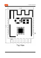
2 Module interfaces 2 Module interfaces 2.1 Dimensions and footprint BPU has 3 lines, 21 pins in total. The spacing of pins at the two sides is 1.4±0.1 mm, and the spacing of pins at the bottom is 1.8±0.1 mm. The dimensions of BPU are 20.3±0.35 mm (L)×15.8±0.35 mm (W) ×3.0±0.15 mm (H). The thickness of the PCB is 1.0±0.
2 Module interfaces 4 / 32
2 Module interfaces 5 / 32
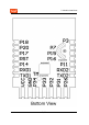
2 Module interfaces 2.
2 Module interfaces Pin number Symbol Pin type Function 6 RXD2 I/O Serial port UART2_RX, which can also be used a common I/O pin and corresponds to P0 of the IC chip 7 TXD2 I/O Serial port UART2_TX, which can also be used a common I/O pin and corresponds to P2 of the IC chip. It can used to output logs.
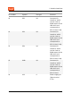
2 Module interfaces Pin number Symbol Pin type Function 10 P32 I/O Common I/O interface, which can be used as PWM output of the LED drive and corresponds to P32 of the IC chip 11 P33 I/O Common I/O interface, which can be used as PWM output of the LED drive and corresponds to P33 of the IC chip 12 P34 I/O Common I/O interface, which can be used as PWM output of the LED drive and corresponds to P34 of the IC chip 13 GND I/O Common I/O interface, which can be used as PWM output of the LED
2 Module interfaces Pin number Symbol Pin type Function 15 TXD1 I/O UART1_TX, which can also be used a common I/O pin and corresponds to P9 of the IC chip 16 RXD1 I/O UART1_RX, which can also be used a common I/O pin and corresponds to P10 of the IC chip 17 P14 I/O ADC port, 12 bit/s, which can also be used as a common I/O interface and corresponds to P14 of the IC chip 18 RESET_N I/O Reset pin (low active), correspond to RESET_N of the IC chip.
2 Module interfaces Pin number Symbol Pin type Function 21 P18 I/O Common I/O interface, which can be used as CS of the SPI interface and corresponds to P18 of the IC chip Test pin TM I Mode selection pin, which is pulled high in burning mode, but pulled down or not connected to anything in other modes. Note: • P indicates a power supply pin and I/O indicates an input/output pin.
3 Electrical parameters 3 Electrical parameters 3.1 Absolute electrical parameters Minimum value Maximum value Unit Parameter Description Ts Storage temperature -65 150 ℃ VCC Power supply voltage -0.3 3.9 V ESD voltage (human body model) TAMB-25℃ - 2 kV ESD voltage (machine model) TAMB-25℃ - 0.5 kV 3.2 Operating conditions Minimum Description value Typical value Maximum value Unit Ta Operating temperature -40 - 105 ℃ VCC Operating voltage 1.8 3.3 3.
3 Electrical parameters Parameter VOH Minimum Description value Typical value Maximum value Unit Voltage output high - VCC V VCC*0.9 3.3 Power consumption in operating mode Maximum value (Typical value) Unit Symbol Conditions Itx Constantly transmit with the output power of 6 dBm 10.9 mA Irx Constantly receive 5.0 mA IDC Average value in mesh networking state 9.4 mA IDC Peak value in mesh networking state 11.
4 RF parameters 4 RF parameters 4.1 Basic RF features Parameter Description Operating frequency 2.4 GHz ISM band Wireless standard Bluetooth LE 5.1 Data transmission rate 1 Mbps Antenna type PCB antenna 4.
4 RF parameters Parameter Co-channel interference suppression Minimum value - Typical value Maximum value Unit -10 - dB 14 / 32
5 Antenna information 5 Antenna information 5.1 Antenna type BPU uses the PCB antenna with a gain of 2.19 dBi. 5.2 Antenna interference reduction To ensure the best RF performance, it is recommended that the antenna be at least 15 mm away from other metal parts. If metal materials are wrapped around the antenna, the wireless signal will be greatly attenuated, thereby deteriorating the RF performance. When designing the finished product, please leave enough space for the antenna.
5 Antenna information 16 / 32
5 Antenna information 17 / 32
6 Packaging information and production instructions 6 Packaging information and production instructions 6.
6 Packaging information and production instructions 19 / 32
6 Packaging information and production instructions The following figure is a schematic diagram of BPU: 20 / 32
6 Packaging information and production instructions Recommended PCB footprint 21 / 32
6 Packaging information and production instructions The default outline dimension tolerance is ±0.35 mm, and the critical dimension tolerance is ±0.1 mm. If you have specific requirements on dimensions, specify them clearly in the datasheet after communication.
6 Packaging information and production instructions 6.2 Production instructions 1. For the modules that can be packaged with the SMT or in an in-line way, you can select either of them according to the PCB design solutions of customers. If a PCB is designed to be SMT-packaged, package the module with the SMT. If a PCB is designed to be in-line-packaged, package the module in an in-line way. After being unpacked, the module must be soldered within 24 hours.
6 Packaging information and production instructions 3. The module needs to be baked in the following cases: • • • • • The packaging bag is damaged before unpacking. There is no humidity indicator card (HIC) in the packaging bag. After unpacking, circles of 10% and above on the HIC become pink. The total exposure time has lasted for over 168 hours since unpacking. More than 12 months has passed since sealing of the bag. 4.
6 Packaging information and production instructions measures. 6. To guarantee the passing rate, it is recommended that you use the SPI and AOI to monitor the quality of solder paste printing and mounting. 6.3 Recommended oven temperature curve Select a proper soldering manner according to the process. For the SMT process, please refer to the recommended oven temperature curve of reflow soldering. For the wave soldering process, please refer to the recommended oven temperature curve of wave soldering.
6 Packaging information and production instructions • D: Ramp-up slope: 1 to 3°C/s • E: Duration of constant temperature: 60 to 120s; the range of constant temperature: 150 to 200°C • F: Duration above the liquidus: 50 to 70s • G: Peak temperature: 235 to 245°C • H: Ramp-down slope: 1 to 4°C/s Note: The above curve is just an example of the solder paste SAC305. For more details about other solder pastes, please refer to Recommended oven temperature curve in the solder paste specifications.
6 Packaging information and production instructions Suggestions on oven temperature curve of wave soldering Suggestions on manual soldering temperature Preheat temperature 80 to 130 °C Soldering temperature 360±20°C Preheat time 75 to 100s Soldering time < 3s/point Peak contact time 3 to 5s NA NA Temperature of tin cylinder 260±5°C NA NA Ramp-up slope ≤2°C/s NA NA Ramp-down slope ≤6°C/s NA NA 27 / 32
6 Packaging information and production instructions 6.
7 MOQ and packaging information 7 MOQ and packaging information Product model MOQ (pcs) Packing method BPU 4400 Tape reel 29 / 32 Modules per reel Reels per carton 1100 4
8 Appendix: Statement 8 Appendix: Statement FCC Caution: Any changes or modifications not expressly approved by the party responsible for compliance could void the user’s authority to operate this device. This device complies with Part 15 of the FCC Rules. Operation is subject to the following two conditions: (1) This device may not cause harmful interference, and (2) this device must accept any interference received, including interference that may cause undesired operation.
8 Appendix: Statement The host product manufacturer is responsible for compliance with any other FCC rules that apply to the host not covered by the modular transmitter grant of certification. The final host product still requires Part 15 Subpart B compliance testing with the modular transmitter installed.
8 Appendix: Statement This product must not be disposed of as normal household waste, in accordance with the EU directive for waste electrical and electronic equipment (WEEE-2012/19/EU). Instead, it should be disposed of by returning it to the point of sale, or a municipal recycling collection point. The device could be used with a separation distance of 20cm to the human body.