ZPU Module Datasheet Version: 20220512 Online Version
Contents Contents 1 Overview 1.1 Features . . . . . . . . . . . . . . . . . . . . . . . . . . . . . . . . . 1.2 Applications . . . . . . . . . . . . . . . . . . . . . . . . . . . . . . . 1.3 Change history . . . . . . . . . . . . . . . . . . . . . . . . . . . . . . 2 2 2 2 2 Module interfaces 2.1 Dimensions and packaging . . . . . . . . . . . . . . . . . . . . . . . 2.2 Pin definition . . . . . . . . . . . . . . . . . . . . . . . . . . . . . . . 3 3 5 3 Electrical parameters 3.
Contents ZPU is a Zigbee module developed by Tuya. It consists of a highly integrated RF processor chip (PHY6222) and a few peripheral circuits. ZPU has an embedded lowpower 32-bit MCU, a 1 MB flash, a 64 KB static random-access memory (SRAM), and 18 I/O pins that support multiplexing.
1 Overview 1 Overview ZPU enables you to build reliable Zigbee products based on your development requirements. 1.1 Features • Built-in low-power 32-bit MCU, which can also be used as an application processor • Operating voltage: 1.8 V to 3.6 V • Peripherals: 5 PWM pins, 2 ADCs, 3 GPIO pins, 2 UARTs, and 1 SPI • Zigbee connectivity – 802.15.4 MAC/PHY – Channels 11 to 26 at 2.405 GHz to 2.
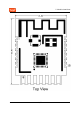
2 Module interfaces 2 Module interfaces 2.1 Dimensions and packaging ZPU has 21 pins arranged in three rows with a spacing of 1.4±0.1 mm between pins on the two sides and a spacing of 1.8±0.1 mm between pins at the bottom. The ZPU dimensions are 20.3±0.35 mm (L) × 15.8±0.35 mm (W) × 3.0±0.15 mm (H). The thickness of the PCB is 1.0±0.1 mm. The following figures show the dimensions and packaging design of the ZPU module.
2 Module interfaces 4 / 32
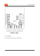
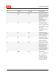
2 Module interfaces 2.2 Pin definition The following table describes the interface pins.
2 Module interfaces No. Symbol I/O type Description 1 P16 I/O Common I/O pin, which can be used as the SCK of the SPI and corresponds to P16 of the IC. 2 P7 I/O Common I/O pin, which can be used as the MOSI of the SPI and corresponds to P7 of the IC. 3 P2 I/O Common I/O pin, which corresponds to P2 of the IC. 4 P3 I/O Common I/O pin, which corresponds to P3 of the IC. 5 P11 I/O The pin for 12-bit ADCs, which can be reused as a common I/O pin and corresponds to P11 of the IC.
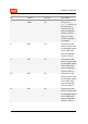
2 Module interfaces No. Symbol I/O type Description 7 TXD2 I/O The pin for UART2_TX, which can be reused as a common I/O pin and corresponds to P15 of the IC. The pin can be used for printing log output. 8 P26 I/O Common I/O pin, which can be used as the PWM output of the LED drive and corresponds to P26 of the IC. 9 P31 I/O Common I/O pin, which can be used as the PWM output of the LED drive and corresponds to P31 of the IC.
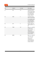
2 Module interfaces No. Symbol I/O type Description 12 P34 I/O Common I/O pin, which can be used as the PWM output of the LED drive and corresponds to P34 of the IC. 13 GND P Common I/O pin, which can be used as the PWM output of the LED drive and corresponds to P26 of the IC. 14 VCC P Power supply pin (Typical value: 3.3 V). 15 TXD1 I/O The UART1_TX pin for sending data, which can be reused as a common I/O pin and corresponds to P9 of the IC.
2 Module interfaces No. Symbol I/O type Description 17 P14 I/O The pin for 12-bit ADCs, which can be reused as a common I/O pin and corresponds to P14 of the IC. 18 RST I/O Hardware reset pin (active at a low level), which corresponds to RESET_N of the IC. 19 P17 I/O Common I/O pin, which corresponds to P17 of the IC. 20 P20 I/O Common I/O pin, which can be used as the MISO of the SPI and corresponds to P20 of the IC.
2 Module interfaces :::info • P indicates a power supply pin. I/O indicates an input/output pin. • If you have special requirements for light colors controlled by the PWM output, contact our business manager.
3 Electrical parameters 3 Electrical parameters 3.1 Absolute electrical parameters Minimum value Maximum value Unit Parameter Description Ts Storage temperature -65 150 °C VCC Power supply voltage -0.3 3.9 V Static electricity voltage (human body model) TAMB -25°C - 2 kV Static electricity voltage (machine model) TAMB -25°C - 0.5 kV 3.
3 Electrical parameters Minimum value Typical value Maximum value Unit Parameter Description VIH I/O high-level input VCC × 0.7 - VCC V VOL I/O low-level output VSS - VCC × 0.1 V VOH I/O high-level output VCC × 0.9 - VCC V 3.3 Power consumption in working mode Transmit power/Re- Average ceive value Peak value (Typical value) Unit Working status Mode Rate Transmit - 250 kbit/s +6 dBm 9.5 14 mA Receive - 250 kbit/s Constantly 7.5 receive 14 mA 3.
3 Electrical parameters Working mode Working status (Ta = 25°C) Average value Peak value (Typical value) Unit Connected The module is in the connected state. 7 14 mA Weakly connected The module is weakly connected. 9.5 21 mA Deep sleep The module is in deep sleep mode, with the 64 KB SRAM remaining active.
4 RF parameters 4 RF parameters 4.1 Basic RF features Parameter Description Working frequency 2.405 to 2.480 GHz Zigbee standard IEEE 802.15.4 Data transmission rate 250 kbit/s Antenna type PCB antenna with a gain of 2.19 dBi 4.
4 RF parameters 4.
5 Antenna information 5 Antenna information 5.1 Antenna type ZPU uses a PCB antenna with a gain of 2.19 dBi. 5.2 Antenna interference reduction To ensure the optimal RF performance, we recommend that the antenna be at least 15 mm away from other metal parts. If metal materials are wrapped around the antenna, the wireless signals will be greatly reduced, deteriorating the RF performance. During the finished product design, sufficient space needs to be reserved for the antenna.
5 Antenna information 17 / 32
6 Packaging information and production instructions 6 Packaging information and production instructions 6.
6 Packaging information and production instructions 19 / 32
6 Packaging information and production instructions ZPU schematic diagram and pin connection: 20 / 32
6 Packaging information and production instructions Recommended PCB footprint: 21 / 32
6 Packaging information and production instructions The default dimensional tolerance is ±0.35 mm and the critical tolerance is ±0.1 mm. If customers have specific requirements on key dimensions, these requirements should be made clear in the datasheet after communication with the customers.
6 Packaging information and production instructions 6.2 Production instructions 1. For the modules that can be packaged with the surface-mount technology (SMT) or in in-line form, you can select either of them according to the PCB design solutions of customers. If a PCB is designed to be SMT-packaged, package the module with the SMT. If a PCB is designed to use an in-line package, use wave soldering. After being unpacked, the module must be soldered within 24 hours.
6 Packaging information and production instructions 3. The module needs to be baked in the following cases: • The vacuum packaging bag is damaged before unpacking. • There is no HIC in the packaging bag. • After unpacking, the HIC indicates a humidity level of 10% or higher (the circle turns pink on the HIC). • The total exposure time has lasted for over 168 hours since unpacking. • More than 12 months have passed since the first sealing of the bag. 4.
6 Packaging information and production instructions 6.3 Recommended oven temperature curve Select a proper soldering technique according to the process. For the SMT process, refer to the recommended oven temperature curve of reflow soldering. For the wave soldering process, refer to the recommended oven temperature curve of wave soldering. There are some differences between the set temperatures and the actual temperature measurements.
6 Packaging information and production instructions • G: Peak temperature: 235°C to 245°C • H: Ramp-down slope: 1°C/s to 4°C/s The curve above is based on solder paste SAC305. For more information about other solder pastes, see the recommended oven temperature curve in the solder paste specifications. Technique 2: Wave soldering process (Oven temperature curve of wave soldering) Set the oven temperatures according to the following temperature curve of wave soldering. The peak temperature is 260°C±5°C.
6 Packaging information and production instructions Suggestions on oven temperature curve of wave soldering Suggestions on manual soldering temperature Peak contact time 3s to 5s N/A N/A Temperature of tin cylinder 260°C±5°C N/A N/A Ramp-up slope ≤ 2°C/s N/A N/A Ramp-down slope ≤ 6°C/s N/A N/A 27 / 32
6 Packaging information and production instructions 6.
7 MOQ and packaging information 7 MOQ and packaging information Product model MOQ (pcs) Shipping packaging method ZPU 4,400 Tape reel 29 / 32 Number of modules per reel Number of reels per carton 1,100 4
8 Appendix: Statement 8 Appendix: Statement FCC Caution: Any changes or modifications not expressly approved by the party responsible for compliance could void the user’s authority to operate this device. This device complies with Part 15 of the FCC Rules. Operation is subject to the following two conditions: (1) This device may not cause harmful interference, and (2) this device must accept any interference received, including interference that may cause undesired operation.
8 Appendix: Statement The host product manufacturer is responsible for compliance with any other FCC rules that apply to the host not covered by the modular transmitter grant of certification. The final host product still requires Part 15 Subpart B compliance testing with the modular transmitter installed.
8 Appendix: Statement This product must not be disposed of as normal household waste, in accordance with the EU Directive for Waste Electrical and Electronic Equipment (WEEE-2012/19/EU). Instead, it should be disposed of by returning it to the point of sale, or to a municipal recycling collection point. The device could be used with a separation distance of 20 cm to the human body.