ZSU-IPEX Module Datasheet Version: 20211115 Online Version
Contents Contents 1 Product overview 1.1 Features . . . . . . . . . . . . . . . . . . . . . . . . . . . . . . . . . 1.2 Applications . . . . . . . . . . . . . . . . . . . . . . . . . . . . . . . 1.3 Change history . . . . . . . . . . . . . . . . . . . . . . . . . . . . . . 2 2 2 3 2 Module interfaces 2.1 Dimensions and footprint . . . . . . . . . . . . . . . . . . . . . . . . 2.2 Pin definition . . . . . . . . . . . . . . . . . . . . . . . . . . . . . . . 4 4 6 3 Electrical parameters 3.
Contents 8 Appendix: Statement 26 II
Contents ZSU-IPEX is a Zigbee module that Tuya has developed. It consists of a highly integrated RF processing chip (EFR32MG21A020F1024IM32-B), a few peripherals, a built-in 802.15.4 PHY/MAC Zigbee network protocol stack and rich library functions.
1 Product overview 1 Product overview ZSU-IPEX is embedded with a low-power 32-bit ARM Cortex-M33 core, 1024-KB flash program memory, 96-KB RAM and abundant peripheral resources. It integrates all function libraries of the Zigbee MAC and TCP/IP. You can develop embedded Zigbee products as required. 1.
1 Product overview 1.3 Change history Update date Updated content 06/30/2021 This is the first release. Version after update V1.0.
2 Module interfaces 2 Module interfaces 2.1 Dimensions and footprint ZSU-IPEX has 3 lines of pins. The spacing of pins at the two sides is 1.4±0.1 mm, and the spacing of pins at the bottom is 1.8±0.1 mm. The dimensions of ZSU-IPEX are 20.3±0.35 mm (L)×15.8±0.35 mm (W) ×3.0±0.15 mm (H).
2 Module interfaces 5 / 28
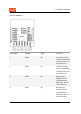
2 Module interfaces 2.
2 Module interfaces Pin number Symbol Type Function 5 PC01 I ADC pin, which corresponds to PC01 (Pin 2) on the internal IC 6 PD03 I/O Common I/O pin, which corresponds to PD03 (Pin 29) on the internal IC 7 PD04 I/O Common I/O pin, which corresponds to PD04 (Pin 28) on the internal IC 8 PB01 I/O Support hardware PWM and correspond to PB01 (Pin 15) on the internal IC 9 PB00 I/O Support hardware PWM and correspond to PB00 (Pin 16) on the internal IC 10 PA00 I/O Support hardware PWM
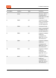
2 Module interfaces Pin number Symbol Type Function 12 PA04 I/O Support hardware PWM and correspond to PA04 (Pin 21) on the internal IC 13 GND P Power supply reference ground 14 VCC P Power supply pin (3.
2 Module interfaces Pin number Symbol Type Function 20 PC02 I/O Common I/O pin, which corresponds to PC02 (Pin 3) on the internal IC 21 PC03 I/O Common I/O pin, which corresponds to PC03 (Pin 4) on the internal IC Note: P indicates a power supply pin and I/O indicates an input/output pin. • Pin 3, 4, 13, 14, and 18 are burning pins, which are not exposed by default. During routing, customers should bypass them.
3 Electrical parameters 3 Electrical parameters 3.1 Absolute electrical parameters Minimum value Maximum value Unit Parameter Description Ts Storage temperature -50 150 ℃ VBAT Power supply voltage 2.0 3.8 V ESD voltage (human body model) TAMB-25℃ - 2 KV ESD voltage (machine model) TAMB-25℃ - 0.5 KV 3.2 Normal working conditions Minimum value Typical value Maximum value Unit Parameter Description Ta Working temperature -40 - 105 ℃ VCC Working voltage 2.0 3.3 3.
3 Electrical parameters Parameter Description VOH I/O high level output Minimum value Typical value Maximum value Unit VDD*0.8 - - V 3.3 TX and RX power consumption Average value Peak value (Typical value) Working status Mode Rate Transmit power/receive Transmit - 250Kbps +20dBm 200 211 mA Transmit - 250 Kbps +10 dBm 62 65 mA Transmit - 250 Kbps +0 dBm 27 29 mA Receive - 250Kbps Constantly 11 receive 15 mA 3.
3 Electrical parameters Working mode Working status, Ta = 25°C Average value Maximum value (Typical value) Unit Connected and idle The module is connected to the network and in idle state.
4 RF parameters 4 RF parameters 4.1 Basic RF features Parameter Description Working frequency 2.405 to 2.480 GHz Zigbee standard IEEE 802.15.4 Data transmission rate 250 Kbps Antenna type IPEX antenna with a gain of 3.1 dBi 4.2 TX performance TX performance Minimum value Typical value Maximum value Unit Output power (250Kbps) -30 15 20 dBm Output power adjustment stepping - 0.
4 RF parameters Parameter PER<8%, RX sensitivity (250 Kbps) Minimum value -102 Typical value Maximum value Unit -101 -99 dBm 14 / 28
5 Antenna information 5 Antenna information 5.1 Antenna type The ZSU-IPEX uses a new generation of IPEX antenna bases. Its structure is shown below: 5.2 Antenna interference reduction It is recommended that the antenna be at least 15 mm away from other metal parts.
6 Packaging information and production instructions 6 Packaging information and production instructions 6.1 Mechanical dimensions The PCB dimensions are 20.3±0.35 mm (W)×15.8±0.35 mm (L) ×1.0±0.1 mm (H).
6 Packaging information and production instructions 6.
6 Packaging information and production instructions 6.
6 Packaging information and production instructions 6.4 Recommended footprint 6.5 Production instructions 1. For the modules that can be packaged with the SMT or in an in-line way, you can select either of them according to the PCB design solutions of customers. If a PCB is designed to be SMT-packaged, package the module with the SMT. If a PCB is designed to be in-line-packaged, package the module in an in-line way. After being unpacked, the module must be soldered within 24 hours.
6 Packaging information and production instructions greater than 10%; or it needs to be packaged again under vacuum and the exposure time needs to be recorded (the total exposure time cannot exceed 168 hours).
6 Packaging information and production instructions • More than 12 months has passed since sealing of the bag. 4.
6 Packaging information and production instructions • A: Temperature axis • B: Time axis • C: Liquidus temperature: 217 to 220°C • D: Ramp-up slope: 1 to 3°C/s • E: Duration of constant temperature: 60 to 120s; the range of constant temperature: 150 to 200°C • F: Duration above the liquidus: 50 to 70s • G: Peak temperature: 235 to 245°C • H: Ramp-down slope: 1 to 4°C/s Note: The above curve is just an example of the solder paste SAC305.
6 Packaging information and production instructions Suggestions on oven temperature curve of wave soldering Suggestions on manual soldering temperature Preheat temperature 80 to 130 °C Soldering temperature 360±20°C Preheat time 75 to 100s Soldering time < 3s/point Peak contact time 3 to 5s NA NA Temperature of tin cylinder 260±5°C NA NA Ramp-up slope ≤2°C/s NA NA Ramp-down slope ≤6°C/s NA NA 23 / 28
6 Packaging information and production instructions 6.
7 MOQ and packaging information 7 MOQ and packaging information Product model MOQ (pcs) Packing method ZSU-IPEX 4400 Tape reel 25 / 28 Modules per reel Reels per carton 1100 4
8 Appendix: Statement 8 Appendix: Statement FCC Caution: Any changes or modifications not expressly approved by the party responsible for compliance could void the user’s authority to operate this device. This device complies with Part 15 of the FCC Rules. Operation is subject to the following two conditions: (1) This device may not cause harmful interference, and (2) this device must accept any interference received, including interference that may cause undesired operation.
8 Appendix: Statement The host product manufacturer is responsible for compliance with any other FCC rules that apply to the host not covered by the modular transmitter grant of certification. The final host product still requires Part 15 Subpart B compliance testing with the modular transmitter installed.
8 Appendix: Statement This product must not be disposed of as normal household waste, in accordance with the EU directive for waste electrical and electronic equipment (WEEE-2012/19/EU). Instead, it should be disposed of by returning it to the point of sale, or to a municipal recycling collection point. The device could be used with a separation distance of 20cm to the human body.