
Maintenance Manual


The other output of the resistive splitter drives U202.
U202 is a buffer amplifier with a gain of about 10 dB. U202
drives the synthesizer prescaler (i.e. it provides a signal to
the PLL).
REFERENCE BUFFER AMPLIFIER
Transistor Q401 and associated components comprise a
buffer amplifier for the reference oscillator signal. (The
reference oscillator signal is produced by the receiver syn-
thesizer module of a MASTR III station.) The 0 dBm refer-
ence oscillator signal is fed through the front panel BNC
connector J1. Resistor R405 provides a 50 ohm load to the
reference oscillator. The output of the Reference Buffer
Amplifier is fed directly to the synthesizer integrated circuit.
The output level at TP9 is approximately 3 volts peak to
peak.
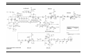
PRESCALER AND SYNTHESIZER
Integrated circuit U402 is the heart of the synthesizer. It
contains the necessary frequency dividers and control cir-
cuitry to synthesize output frequencies by the technique of
dual modulus prescaling. U402 also contains an analog
sample and hold phase detector and a lock detector circuit.
Within the synthesizer (U402) are three programmable
dividers which are loaded serially using the CLOCK, DATA,
and ENABLE inputs (pins 11, 12, and 13 respectively). A
serial data stream (DATA) on pin 12 is shifted into internal
shift registers by low to high transitions on the clock input
(CLOCK) at pin 11. A logic high (ENABLE) on pin 13 then
transfers the program information from the shift registers to
the divider latches.
The reference signal is applied to U402 pin 2 and divided
by the "R" divider. This divides the reference signal down to
a divided reference frequency (Fr). The typical reference
frequency is 12.8 MHz and the typical divided reference
frequency is 5 kHz providing for synthesizer steps of 5 kHz
for use with both 25 kHz and 30 kHz channel spacing. Other
channel spacings are possible by providing proper program-
ming.
The "A" and "N" dividers process the loop feedback
signal provided by the VCO (by way of the dual modulus
prescaler U401). The output of the "N" divider is a divided
version of the VCO output frequency (Fv).
Synthesizer U402 also contains logic circuitry to control
the dual modulus prescaler U401. If the locked synthesizer
output frequency is 150 MHz. The prescaler output nomi-
nally will be equal to 2.34375 MHz (150 MHz/64). This
frequency is further divided down to Fv by the "N" divider
in U402. Fv is then compared with Fr in the phase detector
section.
The phase detector output voltage is proportional to the
phase difference between Fv and Fr. This phase detector
output serves as the loop error signal. This error signal
voltage tunes the VCO to whatever frequency is required to
keep Fv and Fr locked (in phase).
LOOP BUFFER AMPLIFIERS AND LOOP
FILTER
The error signal provided by the phase detector output is
buffered by operational amplifiers (op-amp) U501A and
U501B. The audio modulation signal from U601B is also
applied to the input of U501B. The output of U501B is the
sum of the audio modulation and the buffered error signal.
The output of the second buffer (U501B) is applied to a
loop filter consisting of R506, R507, R508, C505 and C506.
This filter controls the bandwidth and stability of the synthe-
sizer loop. The VHF transmitter synthesizer has a loop
bandwidth of only several Hertz. This is very narrow, result-
ing in an excessively long loop acquisition time. To speed
acquisition, switches U502A and U502C bypass the filter
circuit whenever an ENABLE pulse is received by the Input
Gates.
AUDIO FREQUENCY AMPLIFIER
The transmitter synthesizer audio input line is fed to
U601A. U601A is configured as a unity gain op-amp. Resis-
tor R601 sets the 600 ohm input impedance of this amplifier.
(NOTE: Data for digital modulation is fed to the synthesizer
through the audio input line).
The amplifier output is split into two components and fed
to two variable resistors VR601 and VR602. VR601 sets the
level in the low frequency audio path and VR602 sets the
level in the high frequency audio path. (There is no clear
break between the low and high frequency ranges. All voice
frequencies are within the high frequency range. The low
frequency range contains low frequency data components).
The wiper of VR601 (low frequency path) connects to
the input of U601B, the pre-modulation integrator. U601B
performs the function of a low-pass filter and integrator. The
integrator output is summed with the PLL control voltage at
the input of loop buffer amplifier U501B. This integrated
audio signal phase modulates the VCO. The combination of
pre- integration and phase modulation is equivalent to fre-
quency modulation.
The wiper of VR602 (high frequency path) is connected
to the modulation input of the VCO through C16.
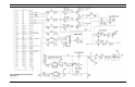
VOLTAGE REGULATORS
U301 and U303 are monolithic voltage regulators (+5
Vdc and -5 Vdc respectively). These two voltages are used
by synthesizer circuitry. The +5 V regulator output is also
used as a voltage reference for the +8 Vdc discrete regulator
circuit.
U302A, Q302 and associated circuitry comprise the +8 volt
regulator. Most module circuitry is powered from the +8 volt
line. The regulator is optimized for especially low noise per-
formance. This is critical because the low noise VCO is pow-
ered by the +8 volt line.
The +8 Vdc line also feeds the +4 Vdc regulator, U302B
and associated resistors. The +4 Vdc regulator provides a bias
voltage for several op-amps in the module.
LOGIC CIRCUITS
Logic circuitry (other than that inside the synthesizer IC -
U402) consists of the following:
•
An address decoder
•
Input gates and level shifters
•
Lock Indicator circuitry
The address decoder, U702, enables the Input Gates when
the A0, A1, and A2 input lines receive the proper logic code
(110 for the transmitter synthesizer). After receiving the proper
code, Y3 (U702-12) sends a logic low signal to U701C. U701C
acts as an inverter and uses the logic high output to turn on
Input Gates U701A, U701B, and U701D. The Input Gates
allow the clock, data and enable information to pass on to the
synthesizer via the level shifters. The Level Shifter Transistors
Q701, Q702 and Q703 convert the 5 volt gate logic level to the
8 volt logic level required by the synthesizer U402.
The Fault Indicator circuitry indicates when the synthe-
sizer is in an out-of-lock condition. The fault detector latches,
U705A and U705B are reset by the enable pulse during initial
loading of data into the synthesizer. If at any time afterwards
the lock detector signal (LD) goes low, the high output of
U705B will cause the output of gates U705C and U705D to go
low. The low output from U705C causes Q704 to turn off, thus
turning on the front panel LED (CR701). The output of U705D
(FLAG) i s connected to J3-13C for external monitoring of the
Synthesizer Module. A logic low on the FLAG line indicates
an out-of-lock condition.
MAINTENANCE
RECOMMENDED TEST EQUIPMENT
The following test equipment is required to test the synthe-
sizer Module:
1. RF signal source for 12.8 MHz, 0 dBm reference (in-
cluded with item 10)
2. AF Generator or Function Generator
3. Modulation Analyzer; HP 8901A, or equivalent, or a
VHF receiver
4. Oscilloscope; 20 MHz
5. DC Meter; 10 meg ohm (for troubleshooting)
6. Power Supply;13.8 Vdc @ 350 mA 12.0 Vdc @ 25
mA
7. Spectrum Analyzer; 0-1 GHz
8. Frequency Counter; 10 MHz - 250 MHz
9. Personal Computer (IBM PC compatible) to load fre-
quency data
10.Service Parts Kit, (TQ0650), (includes software for
loading frequency data)
TEST PROCEDURE
(Steps 5, 6, and 7 can be done using a modulation analyzer
or VHF receiver with 750us de-emphasis switchable in or out.
1. Program synthesizer at 167.5 MHz using the System
Module personality (or Test Software if using RF
Test Fixture TQ-0650).
Verify lock (flag = high)
Verify front panel LED is off.
2. Measure output frequency.
Verify frequency = 167.5000 MHz
±
100 Hz.
3. Measure harmonic content (335 MHz, 502.5MHz).
Verify 2nd harmonic is 30 dBc.
4. Measure RF power output into 50 ohm load.
Verify 10 to 13 dBm (10 to 20 mW).
5. Measure AF distortion with standard modulating sig-
nal input.
Verify <5%.
6. Measure Hum and Noise relative to 0.44 kHz average
deviation, (de-emphasis on).
Verify <-55dB
7. Measure AF response at 300 Hz, 1 kHz (ref) and 3
kHz, (de-emphasis off).
Verify within
±
1.5 dB with respect to 1 kHz refer-
ence.
8. Verify lock at different frequencies.
a. Close switches SW1A and SW1C.
b. Program synthesizer at 156 MHz.
Verify LED is off.
LBI-38640G
2