
Maintenance Manual


c. Open switches SW1A and SW1C and close
switches SW1B and SW1D.
d. Program synthesizer at 147 MHz.
Verify LED is off.
e. Close switches SW1A, SW1B, SW1C and
SW1D.
f. Program synthesizer at 139.5 MHz.
Verify LED is off.
g. Open switches SW1A, SW1B, SW1C and
SW1D.
ALIGNMENT PROCEDURE
1. Set all sections of SW1 to the open position.
2. Apply +13.8 Vdc and -12 Vdc. Verify the current
drain on the 13.8 volt supply is <300 mA and the cur-
rent drain on the -12 volt supply is <20 mA.
3. Program the synthesizer at 175 MHz. Set SW1E and
SW1F (4 possible Combinations = both closed, both
open, E open and F closed, or E closed and F open)
to set V
test
(pin 23A of 96 pin connector) as close to
6.0 volts as possible, but always between 5.5 and 6.5
volts.
4. Program synthesizer at 167.5 MHz for the following
three adjustments
•
Set VR602 for 4.5 kHz peak deviation with a standard
modulating signal applied to the audio input.
•
Set VR601 for 4.4 kHz peak deviation with 1.0 Vrms,
10 Hz sine wave audio applied to module AF input.
•
Apply a 10 Hz 1.4 Vpk square wave (same peak value
as 1.0 Vrms (sine wave) to module AF input. Adjust
VR601 slightly for the flattest demodulated square
wave using a modulation analyzer or receiver (no de-
emphasis) and an oscilloscope . The maximum net
variation in voltage over 1/2 cycle is 10%.
The following service information applies when align-
ing, testing, or troubleshooting the TX Synthesizer:
•
Standard Modulating Signal = 1 kHz sinusoidal
voltage, 1.0 Vrms at the module input terminals
(600 ohm Rin).
•
The input audio level for setting the 4.5 kHz or 10
Hz (or 7 Hz) deviation should always be 1.00
Vrms.
•
In the modulation adjustment, any reference to 0.6
Vrms refers to the voltage level for a STANDARD
signal, or usually 60% (3.0 kHz) of maximum
deviation. The 0.6 Vrms will produce 60% of full
deviation.
•
Logic Levels:
Logic 1 = high = 4.5 to 5.5 Vdc
Logic 0 = Low = 0 to 0.5 Vdc
•
Transmitter Synthesizer Address = A0 A1 A2
= 110
•
Synthesizer data input stream is as follows:
14-bit "R" divider most significant bit (MSB) =
R13 through "R" divider least significant bit
(LSB) = R0
10-bit "N" divider MSB = N9 through "N" divider
LSB = N0
7-bit "A" divider MSB = A6 through "A" divider
LSB = A0
Single high Control bit (last bit)
Latched When Control Bit = 1
DATA ENTRY FORMAT
Latched When
Control Bit = 1
Data in Last A0 ---- A6 N0 ---- N9 R0 ---- R13
Bit LSB MSB LSB MSB LSB
Control Bit
For the transmitter synthesizer, 5 kHz channel
spacing
R=2560
N = integer part of (frequency in kHz) / (320)
A = (frequency in kHz)/(5) - 64*N
All numbers must be converted to binary.
•
ANT_REL line must be logic low (0V) in order to
lock synthesizer.
•
Synthesizer lock is indicated by the extinguishing
of the front panel LED indicator and a logic high
on the fault flag line (J3 pin 1 3C).
•
Always verify synthesizer lock after each new data
loading.
SYMPTOM CHECK INCORRECT READING
(CORRECT READINGS SHOWN) INDICATES DEFECTIVE COMPONENT
SYNTHESIZER FAILS TO LOCK Check DC voltages
+5 V @ U301 Pin 1 U301 or associated components
+8 V @ Q301 collector U302, Q301, Q302 or associated components
- 5 V @ U303 Pin 1 U303 or associated components
Check 12.8 MHz reference signal No reference signal to front panel BNC or
3V P-P, 12.8 MHz @ TP9 or U402 Pin 2 Q401
Check oscillator signal
11.5 1.5 dBm 125 to 180 MHz at Proceed to "Low/No RF output" below
front panel BNC
Check prescaler output
1V P-P, 2.5 MHz @ U401 Pin 4 U202, U401
Check CLOCK, DATA, ENABLE
While loading frequency data into Wrong address or
synthesizer Check 8V logic signals @ U701, U702, Q701, Q702, Q703
Pins 11, 12, 13 of U402
Check Phase detector output
5 kHz random signal @ U501 Pin 7 U402, U501
Low/No RF Output Check oscillator
LESS than 0.5 Vdc @ TP3 or collector Synthesizer not keyed (low on ANT relay line)
of Q101 or Q101, Q102
50 mV, 125 to 180 MHz @ TP4 Q1
No Modulation Check RF chain
0 dBm, 125 to 180 MHz @ TP6 U201
+5 dBm, 125 to 180 MHz @ TP7 U203
11.5
±
1.5 dBm to 180 MHz at front Q201
panel BNC
No Modulation Check AF amplifier
Apply 1V, 1 kHz signal to TX/Audio/ Hi U601
Check 1V signal @ TP12 or U601 Pin 1
TROUBLESHOOTING GUIDE
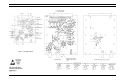
TROUBLESHOOTING
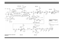
A troubleshooting guide is provided showing typical
measurements at the various test points. The location of the
test points and adjustments are shown in Figure 2.
Perform step 3 only if switch SW1 has been replaced.
Otherwise go to step 4.
NOTE
SERVICE NOTES
LBI-38640G
3