
Inverter Service Manual


3- 1
3.Debug Mode
Additional displays as follows can be seen by turning Debug mode ON (C091 ->1).
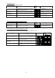
3.1 Monitor mode
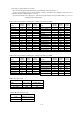
No Functional Display code SJ300/L300P A Monitor or data range
1 Control frequency monitor d101 0.00-99.99/100.0-400.0Hz
2 Direct-current voltage monitor d102 0.0-999.9V
3 BRD on-monitor d103 0.00-99.99/100.0s
4 Electronic thermal monitor d104 0.00-99.99/100.0%
5 Gate array trip factor monitor d105 00-FF
6 MCU No. monitor d106 0000-9999
d101 ( Output frequency monitor (Hz)): Monitor of the output frequency of the inverter.
d102 ( DC bus voltage monitor (V)): Monitor of the DC bus voltage (VPN) of the inverter.
d103 ( BRD ON monitor (s)): There is an integrated BRD circuit on 11kW and less for SJ300, and 15kW and less
for L300P series. You can find accumulated turning ON time for the integrated BRD
transistor.
d104 ( Electronic thermal monitor (%)):You can find the usage ratio of electronic thermal performance as %.
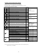
d105 (Trip cause monitor of gate array):There are 8 items of trips which are detected by the internal gate array
and these items are transmitted to MCU.
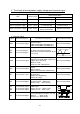
Bit7 bit6 Bit5 bit4 bit3 bit2 bit1 bit0
Contents of d105 are expressed in HEX.
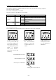
(Example 1)
20
20 (HEX) = 00100000 (BIN)
bit5 = “1” -> IGBT error (V phase)
(Example 1)
62
62 (HEX) = 01100010 (BIN)
bit1, bit5, bit6 = “1” -> IGBT error (U, V, W phase)
d106(MCU No monitor): Display the software management number of MCU incorporated.
IGBT error
W phase
(E30)
IGBT error
V phase
(E30)
IGBT error
U phase
(E30)
Gate array
error
(E23)
Over
temperature
(E21)
Over voltage
(E07)
Under voltage
(E09)
Option
Ground fault
(E14)