SJ-EN Ethernet Communications Option Board Instruction Manual • SJ300 Series • L300P Series NOTE: REFER ALSO TO SJ300 or L300P SERIES INSTRUCTION MANUAL Manual Number: HAL1051 December 2004 After reading this manual, keep it handy for future reference. Hitachi America, Ltd.
NOTES:
Table of Contents Table of Contents Table of Contents................................................................................................................... 3 Chapter 1 – General Description .......................................................................................... 5 Chapter 2 – Installation and Wiring...................................................................................... 9 Chapter 3 – Configuration..................................................................
Table of Contents NOTES: Page 4 of 36
Chapter 1 Chapter 1 – General Description The SJ-EN option board is an Ethernet communication interface for the Hitachi SJ300 and L300P series of AC Variable Frequency Inverters. The board can be installed in one of the two available option slots in the inverter. The SJ-EN uses the open MODBUS/TCP communication protocol. It utilizes a 10Base-T physical interface with a 10 Mbps data transfer rate.
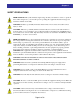
Chapter 1 SAFETY PRECAUTIONS HIGH VOLTAGE: This symbol indicates high voltage. It calls your attention to items or operations that could be dangerous to you and other persons operating this equipment. Read the message and follow the instructions carefully. WARNING: Indicates a potentially hazardous situation that, if not avoided, can result in serious injury or death.
Chapter 1 CAUTION: Be sure not to touch the surface or terminals of the SJ-EN Ethernet option board while the inverter is energized; otherwise there is the danger of electric shock. CAUTION: The software lock modes described in the SJ300 inverter manual are NOT supported via the SJ-EN option board. This means that network commands can bypass any software lock settings configured via the inverter keypad. It is incumbent on the user to make sure no safety lockouts are violated through network commands.
Chapter 1 NOTES: Page 8 of 36
Chapter 2 Chapter 2 – Installation and Wiring Orientation to Product Features Figure 2-1 below shows the physical layout of the SJ-EN Ethernet option board. In particular, note the location of status LEDs and DIP-switches. STATUS LEDs • • • • STATUS LINK ACTIVITY ERROR Connector to connect to SJ300 or L300P (rear of board) RJ45 Jack 7 6 5 4 3 2 1 0 SJ-EN DIP Switches ON RXD LED OFF TXD LED Figure 2-1 SJ-EN Layout The pinout for the RJ45 connector is as follows: 1. 2. 3. 4. 5. 6. 7. 8.
Chapter 2 Installing the Option Board Power down the inverter and wait at least five minutes before moving to the next step. Open and remove the lower terminal cover. Confirm that the red CHARGE LED is extinguished and that the DC bus is fully discharged before proceeding further, otherwise there is the danger of electric shock. Then remove keypad from the inverter. You can now remove the upper front cover to expose the two option ports inside.
Chapter 2 User Interface The SJ-EN has six LEDs to convey module status and activity. Four LEDs next to the RJ45 connector: • STATUS (GREEN) – This LED will be ON whenever the SJ-EN is receiving proper power from the inverter and the self diagnostics have shown the board to be functioning normally. • LINK (GREEN) – This LED is ON when the SJ-EN is receiving valid Ethernet pulses. • ACTIVITY (GREEN) – This LED is ON whenever there is Ethernet traffic in the cable.
Chapter 2 NOTES: Page 12 of 36
Chapter 3 Chapter 3 – Configuration Install NetEdit3 Software NetEdit3 Software is provided on the CD-R enclosed with the SJ-EN option board. This software is required to configure the board. It can also be used to update the SJ-EN firmware in the event of a future update. NetEdit3 is compatible with Microsoft® Windows® 98, Windows ME, Windows 2000, Windows XP, and Windows NT4. In Windows, run the program “SetupNE3.exe” on the CD-R to install the program.
Chapter 3 Figure 3-1 NetEdit3 Initial Screen The NetEdit3 software should find and list any SJ-EN attached to the network. If not, just click on “Scan Network”. An entry will appear in the Device List (grid area), with the board details as shown in Figure 3-2. If more than one board is connected in a common network, you will see a line entry for each of them. The “Module Info” and “General Settings” tabs will now also appear next to the “General Help” tab, below the Device List.
Chapter 3 Figure 3-2 NetEdit3 Screen after Scan of Network Figure 3-3 NetEdit3 General Settings Dialog Box Page 15 of 36
Chapter 3 NOTES: Page 16 of 36
Chapter 4 Chapter 4 – Operation Setting Up the Inverter for Ethernet Network Operation Once the SJ-EN board has been properly configured and connected to a network as described in Chapter 3, it is capable of reading data from and writing data to the inverter. However if it is desired to have either the RUN command and/or the speed reference come from the Ethernet master, you must change two inverter parameters as shown in the following table.
Chapter 4 NOTES: Page 18 of 36
Chapter 5 Chapter 5 – Troubleshooting In general, the first step to troubleshooting should be to inspect the status LEDs on the SJ-EN board, in addition to the inverter operator/keypad display. These will give valuable clues to the nature of the problem. In addition, the inverter operator/keypad will provide diagnostic information for certain types of errors. Error codes for the option boards will have the format of: E6X.X for a board installed in option slot 1, or E7X.
Appendix NOTES: Page 20 of 36
Appendix Appendix – Parameter List Note: Parameters in BOLDFACE can be edited while inverter is in the RUN mode. “RO” means the parameter is Read Only, and “R/W” means the value can be read or written.
Appendix D367 3733 3734 Frequency at Trip 3 X100 RO 0 – 40000 D368 3735 3736 Output current at Trip3 X10 RO 0 – 10000 D369 3737 3738 PN voltage (DC voltage) at Trip 3 X10 RO 0 – 10000 D370 3739 3740 Cumulative RUN time at Trip 3 X1 RO 0– 4294836225 D371 3741 3742 Cumulative power–on time at Trip 3 X1 RO 0– 4294836225 D084 3167 3168 Error Code of Trip 4 X1 RO 0 – 255 D373 3745 3746 Frequency at Trip 4 X100 RO 0 – 40000 D374 3747 3748 Output current at Trip
Appendix F – Main Profile Functions F001 4001 4002 Output frequency setting(Hz) / PID Setpoint (%) X1000 RO 0 – 400000 F002 4003 4004 Acceleration time 1 X100 R/W 1 – 360000 motor X100 R/W 1 – 360000 F202 4403 4404 Acceleration time 1, 2 nd rd F302 4603 4604 Acceleration time 1, 3 motor X100 R/W 1 – 360000 F003 4005 4006 Deceleration time 1 X100 R/W 1 – 360000 nd F203 4405 4406 Deceleration time 1, 2 motor X100 R/W 1 – 360000 F303 4605 4606 Deceleration time
Appendix A022 43 44 Multi–speed frequency 2 X100 R/W 0 – 40000 A023 45 46 Multi–speed frequency 3 X100 R/W 0 – 40000 A024 47 48 Multi–speed frequency 4 X100 R/W 0 – 40000 A025 49 50 Multi–speed frequency 5 X100 R/W 0 – 40000 A026 51 52 Multi–speed frequency 6 X100 R/W 0 – 40000 A027 53 54 Multi–speed frequency 7 X100 R/W 0 – 40000 A028 55 56 Multi–speed frequency 8 X100 R/W 0 – 40000 A029 57 58 Multi–speed frequency 9 X100 R/W 0 – 40000 A030 59 60 M
Appendix A057 113 114 DC braking force for starting X1 R/W 0 – 100 * A058 115 116 DC braking time for starting X10 R/W 0 – 600 A059 117 118 DC braking carrier frequency X10 R/W 5 – 150 * A061 121 122 Frequency upper limit setting X100 R/W 0 – 40000 X100 R/W 0 – 40000 X100 R/W 0 – 40000 X100 R/W 0 – 40000 A261 521 522 Frequency upper limit setting, 2 motor A062 123 124 Frequency lower limit setting nd nd A262 523 524 Frequency lower limit setting, 2 motor A0
Appendix A094 187 188 Select method to switch to acc2/dec2 profile X1 R/W 0–1 A294 587 588 Select method to switch to acc2/dec2 profile, 2nd motor X1 R/W 0–1 A095 189 190 Acc1 to Acc2 frequency transition point X100 R/W 0 – 40000 A295 589 590 Acc1 to Acc2 frequency transition point, 2nd motor X100 R/W 0 – 40000 A096 191 192 Dec1 to Dec2 frequency transition point X100 R/W 0 – 40000 A296 591 592 Dec1 to Dec2 frequency transition point, 2nd motor X100 R/W 0 – 40000 A0
Appendix B006 1011 1012 Phase loss detection enable X1 R/W 0–1 B007 1013 1014 Restart frequency threshold X100 R/W 0 – 40000 B012 1023 1024 Level of electronic thermal setting, 1st motor X10 R/W 200 – 1200 B212 1423 1424 Level of electronic thermal setting, 2nd motor X10 R/W 200 – 1200 B312 1623 1624 Level of electronic thermal setting, 3rd motor X10 R/W 200 – 1200 B013 1025 1026 Electronic thermal characteristic, 1st motor X1 R/W 0–2 B213 1425 1426 Electronic th
Appendix B045 1089 1090 Torque limit LADSTOP enable X1 R/W 0–1 B046 1091 1092 Reverse run protection enable X1 R/W 0–1 B050 1099 1100 Controlled deceleration and stop on power loss X1 R/W 0–1 B051 1101 1102 DC bus voltage trigger level during power loss X10 R/W 0 – 10000 B052 1103 1104 Over–voltage threshold during power loss X10 R/W 0 – 10000 B053 1105 1106 Deceleration time setting during power loss X100 R/W 1 – 360000 B054 1107 1108 Initial output frequency de
Appendix B113 1225 1226 Free V/F control voltage 7 X10 R/W 0 – 8000 B120 1239 1240 Brake control enable X1 R/W 0–1 B121 1241 1242 Brake wait time for release X100 R/W 0 – 500 B122 1243 1244 Brake wait time for acceleration X100 R/W 0 – 500 B123 1245 1246 Brake wait time for stopping X100 R/W 0 – 500 B124 1247 1248 Brake wait time for confirmation X100 R/W 0 – 500 B125 1249 1250 Brake release frequency setting X100 R/W 0 – 40000 B126 1251 1252 Brake release
Appendix C034 2067 2068 Intelligent output 14 active state X1 R/W 0–1 C035 2069 2070 Intelligent output 15 active state X1 R/W 0–1 C036 2071 2072 Alarm relay output active state X1 R/W 0–1 C040 2079 2080 Overload signal output mode X1 R/W 0–1 C041 2081 2082 Overload level setting X10 R/W 0 – 2000 C042 2083 2084 Frequency arrival setting for acceleration X100 R/W 0 – 40000 C043 2085 2086 Arrival frequency setting for deceleration X100 R/W 0 – 40000 C044 2087
Appendix C123 2245 2246 [O2] input zero calibration X1 R/W 0 – 65535 C195 2389 2390 Region code selection X1 RO 0–2 C196 2391 2392 Capacity code selection X1 RO 1 – 15 * C197 2393 2394 Voltage code selection X1 RO 0–1 C198 2395 2396 Inverter model series code X1 RO 0–1 X1 R/W 0–2 H – Motor Constants and Functions H001 5001 5002 Auto–tuning setting st H002 5003 5004 Motor data selection, 1 motor X1 R/W 0–2 H202 5403 5404 Motor data selection, 2nd motor X1
Appendix H034 H234 H050 H250 H051 H251 5067 5467 5099 5499 5101 5501 5068 Inertia J, 1st motor (Auto) X1000 R/W 1 – 9999000 X1000 R/W 1 – 9999000 X10 R/W 0 – 10000 X10 R/W 0 – 10000 X10 R/W 0 – 10000 motor X10 R/W 0 – 10000 st st 5468 Inertia J, 1 motor (Auto) 5100 st 5500 5102 5502 PI proportional gain, 1 motor PI proportional gain, 2 nd motor st PI integral gain, 1 motor PI integral gain, 2 nd H052 5103 5104 P Proportional gain, 1 motor X100 R/W 1 – 1000 H252 55
Appendix P – Expansion Card Functions P001 6001 6002 Selection of action at option1 error X1 R/W 0–1 P002 6003 6004 Selection of action at option2 error X1 R/W 0–1 P010 6019 6020 Feedback option enable X1 R/W 0–1 P011 6021 6022 Encoder PPR setting X1 R/W 128 – 65000 P012 6023 6024 Control pulse setting X1 R/W 0–1 P013 6025 6026 Pulse input mode setting X1 R/W 0–3 P014 6027 6028 Home search stop position setting X1 R/W 0 – 4095 P015 6029 6030 Home search s
Appendix R – Reference Codes R001 7001 7002 Status of Inverter X1 RO 0 – 360000 R002 7003 7004 Set Frequency X1 RO 0 – 360000 R004 7007 7008 Output Frequency X1 RO 0 – 360000 R005 7009 7010 Commanded direction of rotation X1 R/W 0–2 R006 7011 7012 Direction of output rotation X1 RO 0 – 360000 R007 7013 7014 Output terminals data X1 RO 0 – 360000 R008 7015 7016 Upper data of input terminals X1 RO 0 – 360000 R010 7019 7020 Lower data of input terminal X1
Index Index A I A - Standard Functions · 23 Activity LED · 11 address, Ethernet · 14 Installing · 10 Interface, User · 11 IP address · 14 B K B - Fine-Tuning Functions · 26 keypad, inverter · 19 C L C - Intelligent Terminal Functions · 29 cable, Ethernet · 13 Carton Contents · 5 Compatibility, Inverter · 7 Configuration · 13 layout, board · 9 LEDs · 9, 11, 13 Link LED · 11 D MODBUS Functions, supported · 17 module ID · 13, 14 M D - Monitoring Functions · 21 device ID · 13 DIP-switches · 9, 1
Index R Status LED · 11 R - Reference Codes · 34 Registers, reading and writing · 17 RJ45 connector · 9 RXD LED · 11 T S W Safety Precautions · 6 software · 13 Warranty · 5 Wiring · 9 Troubleshooting · 19 TXD LED · 11 Page 36 of 36