
Information
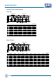


Improper circuit layout and pad/land size may cause poor solder joints between the component and the
PC board. Insufficient solder may create a weak joint, and excessive solder may increase the potential for
mechanical or thermal cracks in the ceramic capacitor. Therefore we recommend the solder pad/land size
to be as shown in the following table:
1. Size and recommend land dimensions for reflow soldering
EIA Code
Chip (mm) Land (mm)
L W A B C D E
0201 0.60 0.30 0.2~0.3 0.2~0.4 0.2~0.4 -- --
0402 1.00 0.50 0.3~0.5 0.3~0.5 0.4~0.6 -- --
0603 1.60 0.80 0.4~0.6 0.6~0.7 0.6~0.8 -- --
0805 2.00 1.25 0.7~0.9 0.6~0.8 0.8~1.1 -- --
1206 3.20 1.60 2.2~2.4 0.8~0.9 1.0~1.4 1.0~2.0 3.2~3.7
1210 3.20 2.50 2.2~2.4 1.0~1.2 1.8~2.3 1.0~2.0 4.1~4.6
1808 4.60 2.00 2.8~3.4 1.8~2.0 1.5~1.8 1.0~2.8 3.6~4.1
1812 4.60 3.20 2.8~3.4 1.8~2.0 2.3~3.0 1.0~2.8 4.8~5.3
1825 4.60 6.35 2.8~3.4 1.8~2.0 5.1~5.8 1.0~4.0 7.1~8.3
2208 5.70 2.00 4.0~4.6 2.0~2.2 1.5~1.8 1.0~4.0 3.6~4.1
2211 5.70 2.80 4.0~4.6 2.0~2.2 2.0~2.6 1.0~4.0 4.4~4.9
2220 5.70 5.00 4.0~4.6 2.0~2.2 3.5~4.8 1.0~4.0 6.6~7.1
2225 5.70 6.35 4.0~4.6 2.0~2.2 5.1~5.8 1.0~4.0 7.1~8.3
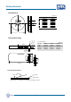
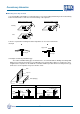
2. Mechanical strength varies according to location of chip capacitors on the P.C. board.
Design the layout of components on the PC board in such a way to minimize the stress imposed on
the components, upon flexure of the boards in depanelization or other processes.
Component layout close to the edge of the board or the
“depanelization line” is not recommended.
Susceptibility to stress is in the order of: a>b>c and d>e
a
c
b
d
slit
perforation
e
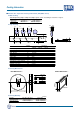
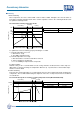
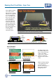
In the pick and place operation, if the low dead point is too low, excessive stress is applied to
component. This may cause cracks in the ceramic capacitor, therefore it is required to move the low
dead point of the nozzle to the higher level to minimize the board warpage and stress on the
components. Nozzle pressure should be adjusted to N to 3N (static load) during the pick and place
operation.
1. Sometimes cracking can be caused by the impact load of the pick and place nozzle.
Nozzle
Crack
Excessive Stress Warping of Board
PCB
Warping of Board
Support pin
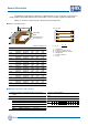
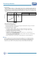
2. Amount of Adhesive
a
a
b
c
c
Example : 0805 & 1206
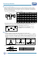
Construction of Board Pattern
Mounting
E
Land
A
Solder Resistor
C
B
Capacitor
D
Slit
Precautionary Information
Holy Stone
a 0.2mm min.
b 70 ~ 100
m
c Do not touch the solder land
- 54 -