
Product Specs


Page 13
nRF51802 Product Specification v1.2
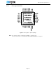
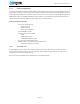
2.2.2.1 Pin functions QFN32
Pin Pin name Pin function Description
1
VDD Power Power supply.
2
DCC Power DC/DC output voltage to external LC filter.
3
P0.00
AREF0
Digital I/O
Analog input
General purpose I/O pin.
ADC/LPCOMP reference input 0.
4
P0.02
AIN3
Digital I/O
Analog input
General purpose I/O pin.
ADC/LPCOMP input 3.
5
P0.03
AIN4
Digital I/O
Analog input
General purpose I/O pin.
ADC/LPCOMP input 4.
6
P0.04
AIN5
Digital I/O
Analog input
General purpose I/O pin.
ADC/LPCOMP input 5.
7
P0.06
AIN7
AREF1
Digital I/O
Analog input
Analog input
General purpose I/O pin.
ADC/LPCOMP input 7.
ADC/LPCOMP reference input 1.
8
VDD Power Power supply.
9
VSS Power
Ground (0 V)
1
.
10
P0.08 Digital I/O General purpose I/O pin.
11
P0.09 Digital I/O General purpose I/O pin.
12
P0.12 Digital I/O General purpose I/O pin.
13
P0.14 Digital I/O General purpose I/O pin.
14
P0.16 Digital I/O General purpose I/O pin.
15
SWDIO/nRESET Digital I/O
System reset (active low). Also hardware debug and flash
programming I/O.
16
SWDCLK Digital input Hardware debug and flash programming I/O.
17
P0.17 Digital I/O General purpose I/O pin.
18
DEC2 Power Power supply decoupling.
19
VDD_PA Power output Power supply output (+1.6 V) for on-chip RF power amp.
20
ANT1 RF Differential antenna connection (TX and RX).
21
ANT2 RF Differential antenna connection (TX and RX).
22
VSS Power Ground (0 V).
23
VSS Power Ground (0 V).
24
AVDD Power Analog power supply (Radio).
25
XC1 Analog input
Connection for 16/32 MHz crystal or external 16 MHz clock
reference.
26
XC2 Analog output Connection for 16/32 MHz crystal.
27
DEC1 Power Power supply decoupling.