
User's Manual


6
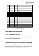
the IC
4
P1.6
I/O
RESERVED, P1.6, which is connected to P1.6 on
the IC
5
P0.1
I/O
RESERVED ,P0.1, which is connected to P0.1 on
the IC
6
P0.6
I/O
RESERVED, P0.6, which is connected to P0.6 on
the IC
7
NC
I/O
Serial peripheral interface clock pin
8
GND
P
Power supply reference ground pin
9
RXD
I/O
UART_RX, which is connected to P0.4 on the IC
10
TXD
Output
UART_TX, which is connected to P0.3 on the IC
11
GND
P
Power supply reference ground pin
12
VCC
P
Power supply pin
13
PRG
I/O
Set high to enter flash programming mode
14
SCK
I/O
Serial peripheral interface clock pin
15
RST
I/O
Hardware reset pin (active at a low level)
16
GPIO
I/O
Reserved
17
MI
I/O
Reserved
18
SCN
I/O
Reserved
19
GND
P
Power supply reference ground pin
20
GND
P
Power supply reference ground pin
Table 1 HM2401 interface pins
3. Integration Instructions
3.1 List of applicable FCC rules
This module has been tested and found to comply with part 15.247, and
RSS-247 requirements for Modular Approval.
3.2 Summarize the specific operational use conditions
This module can be used in DTU, micro-converter and other equipment. The
input voltage to the module should be nominally 1.9~3.6 VDC ( typical 3.3VDC) .
The ambient temperature of the module should not exceed 80℃.