T M 1 1 - 6 6 2 5 - 2 9 5 8 - 1 4 & P TECHNICAL MANUAL OPERATOR’S, ORGANIZATIONAL, DIRECT SUPPORT AND GENERAL SUPPORT MAINTENANCE MANUAL (INCLUDING REPAIR PARTS AND SPECIAL TOOLS LIST) FOR POWER SUPPLY PP-7545/U (HEWLETT-PACKARD MODEL 6269B) (NSN 6130-00-148-1796) HEADQUARTERS, DEPARTMENT OF THE ARMY 21 AUGUST 1980
S A F E T Y S T E P S I S V I C T I M DO T H E NOT TRY IF POSSIBLE IF YOU TO , PULL, SAFETY USING SOME SEND OTHER FOR AFTER SHOCK, OR THE OFF AS T H E THE S O M E O N E OR LIFT SOON INDIVIDUAL POWER ELECTRICAL THE POLE PERSON OR A TO ROPE OR MATERIAL AS PERSON S O U R C E PERSON IMMEDIATELY THE S H O C K ELECTRICAL THE INSULATING W I T H RESUSCITATION GRAB WOODEN INJURED MOVE AND TURN I F E L E C T R I C A L OFF PUSH, HELP THE C O N T A C T
This manual includes copyright material reproduced by permission of the HEWLETT-PACKARD Company. TM 11-6625-2958-14&P TECHNICAL MANUAL No.
TABLE OF CONTENTS Section 0 I II III Page No. INSTRUCTIONS . . . . . . . . . . . . . . . 6-1 0-1 Scope 0-1 0-2 Indexes of Publications 0 - 1 0-3 Forms and Records 0-1 0-4 Reporting Equipment Improvement Recommendations (EIR) 0-1 0-1 0-5 Administrative Storage 0-6 Destruction of Army Electronics Materiel 0-1 GENERAL INFORMATION. . . . . . . . 1-1 Description 1-7 Specifications 1-9 Options 1-11 Instrument/Manual Identification 1-14 Ordering Additional Manuals INSTALLATION . . . . . . . .
TABLE OF CONTENTS (Continued) Section Page No. V MAINTANCE . . Continued 5-103 Preregulator Tracking (5 O and 60Hz Operation) 5-21 5-105 50Hz Operation (Option 005) 5-21 5-107 Crowbar Trip Voltage 5-21 5-109 Maximum Crowbar Trip Voltage 5-22 APPENDIX A. B. Section APPENDIX Section I. II. III. c. D. I . II. 111. Iv. Section 5-111 Crowbar Disablement Page No. 5-22 VI REPLACEABLE PARTS . . . . . . . . . . . ...
LIST OF ILLUSTRATIONS Page No. Figure 1-1 DC Power Supply, Model 6259B, 6260B, 6261B, 6268B, or 6269B . . . . . . . . . . . .. l-l 2-1 Outline Diagram . . . . . . . . . . .. . . . . . . . . . . . . . . . . . . . . . . . . . . . . . . . . . . . . . . . . . . . 2-1 2-2 Bias Transformer Primary Connections for 208Vac and 115Vac Operation . . . . . . .2-2 2-3 Power Transformer Primary Connections for 208Vac and 115Vac Operation . . . ...2-2 2-4 Power Transformer T1 Primary Connections for 208Vac Operation. . .
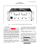
TM 11-6625-2958-14&P SECTION O INTRODUCTION 0-1. SCOPE. a. This manual describes DC Power Supply PP-7545/U (fig. l-l) and provides maintenance instructions. Throughout this manual, PP-7545/U is referred to as the Hewlett-Packard (HP) Model 6269B DC Power supply. 0-2. INDEXES OF PUBLICATIONS. . 4430.3E and DSAR 4140.55. c. Discrepancy in Shipment Report (DISREP) (SF 361). Fill out and forward Discrepancy in Shipment Report (DISREP) (SF 361) as prescribed in AR 55-38/NAVSUPlNST 4610.33B/AFR 7518\MCO P4610.
TM 1 1 - 6 6 2 5 - 2 9 5 8 - 1 4 & P SECTION I GENERAL INFORMATION Figure 1-1. DC Power Supply, Model 6259B, 6260B, 6261B, 6268B, or 6269B 1-1 DESCRIPTION 1-2 This power supply, Figure 1-1, is completely transistorized and suitable for either bench or relay rack operation. It is a well-regulated, constant voltage/constant current supply that will furnish full rated output voltage at the maximum rated output current or can be continuously adjusted throughout the output range.
TM 11-6625-2958-14&P may be used in series when a higher output voltage is required in the constant voltage mode of operat ion or when greater voltage compliance is required in the constant current mode of operation. AutoSeries operation permits one-knob control of the total output voltage from a “master” supply. d. Auto-Parallel Operation. The power supply may be operated in parallel with a similar unit when greater output current capability is required.
TM 11-6625-2958-14&P your local Hewlett-Packard field office (see list at rear of this manual for addresses). Specify the model number, serial number prefix, and HP part number shown on the title page. 1-14 ORDERING ADDITIONAL MANUALS 1-15 One manual is shipped with each power supply. Additional manuals may be purchased from Table 1-1. Specifications INPUT: 230Vac *10%, single phase, 57-63 Hz, 18A, 2500W @ 230V. METERS: A front panel voltmeter (0-50V) and ammeter (0-60A) is provided.
TM 1 1 - 6 6 2 5 - 2 9 5 8 - 1 4 & P SECTION II INSTALLATION 2-1 INITIAL INSPECTION 2-2 Before shipment, this instrument was inspected and found to be free of mechanical and electrical defects. As soon as the instrument is unpacked, inspect for any damage that may have occurred in transit. Save all packing materials until the inspection is completed. If damage is found, file a claim with the carrier immediately. HewlettPackard Sales and Service office should be notified.
TM 11-6625-2958-14&P transformer (see Figure 2-2 B). Leave wire from fan B2 (not used in 62599) soldered to “230V” terminal. c. Re-install RFI assembly by reversing procedure of Step (a). d. Unsolder wire connected to terminal 5 of power transformer T1 (see Figure 7-4) and solder it instead to terminal 4 of transformer (see Figure 2-3 B). Figure 2-3. Power Transformer Primary Connections for 208Vac and 115Vac Operation . (Model 6259B, 6261B, and 6268B) Figure 2-2.
TM 11-6625-2958-14&P Figure 2-4. Power Transformer T 1 Primary Connections for 208Vac Operation (Model 6260B and 6269B) of power transformer T1 (see Figure 7-4) and solder it instead to "208V" terminal of transformer (see Figure 2-4 B). Figure 2-5.
TM 11-6625-2958-14&P b. Perform Steps (b) through (e) of Paragraph 2-22. grounded) and be of sufficient wire size to handle the input current drawn by the supply (see Paragraph 2-16). Note that when the supply is operated from a 115Vac source, the input current is approximately double that shown in Paragraph 2-16.
TM 1 1 - 6 6 2 5 - 2 9 5 8 - 1 4 & P SECTION Ill OPERATING INSTRUCTIONS Figure 3-1. Front Panel Controls and Indicators,’ Modal 6259B, 6260B, 6261B, 6268B or 6269B 3-1 TURN-ON CHECKOUT PROCEDURE 3-3 OPERATING MODES 3-2 The following checkout procedure describes the use of the front panal controls and indicators (Figure 3-1) and ensures that the supply is operational. a. Set LINE circuit breaker ① to ON, and observe that pilot light ② lights. b.
TM 11-6625-2958-14&P Clockwise rotation of the control produces higher trip voltages. The factory sets the control fully clockwise. The crowbar may be disabled completely if desired. (Refer to Paragraph 5-11 1.) Figure 3-2. 3-13 False crowbar tripping must be considered when adjusting the trip point. If the trip voltage is set too close to the operating output voltage of the supply, a transient in the output will falsely trip the crowbar.
TM 11-6625-2958-14&P 3-26 The output voltage of the supply should be -15mV ±5mV when zero ohms is connected across the programming terminals. If a zero ohm voltage closer to zero than this is required, it may be achieved by inserting and adjusting R110 as discussed in Paragraph 5-83, or, if the instrument is equipped with Option 020, by adjusting potentiometer R113 as discussed in Paragraph 5-85. then proceed at a slower rate towards zero.
TM 11-6625-2958-14&P Figure 3-6. Remote Resistance Programming (Constant Current) Figure 3-5. Remote Voltage Programming, Non-Unity Gain (Constant Voltage) with Option 021, by adjusting potentiometer R116 as discussed in Paragraph 5-98.
TM 11-6625-2958-14&P programmed using an external voltage source with variable gain by utilizing the strapping pattern shown in Figure 3-8. In this mode, the output current is found by multiplying the external voltage source (Es) by [Rp/(RR x Kp)], where Kp is the constant current voltage programming coefficient as given in Paragraph 3-37. The value of reference resistor RR and programming voltage source Es should be such that the value of ES /RR is equal to or greater than 2.5mA. Figure 3-7.
TM 11-6625-2958-14&P 3-43 For reasonable load lead lengths, remote sensing greatly improves the performance of the supply. However, if the load is located a considerable distance from the supply, added precautions must be observed to obtain satisfactory operation. Notice that the voltage drop in the load leads subtracts directly from the available output voltage and also reduces the amplitude of the feedback error signals that are deveIoped within the unit.
TM 11-6625-2958-14&P current greater than that available from one supply. Auto-Parallel operation permits equal current sharing under all load conditions, and allows complete control of the output current from one master power supply. The output current of each slave will be approximately equal to the master’s output current regardless of the load conditions.
TM 11-6625-2958-14&P on the maximum voltage rating of the "master" supply. The value of RX is this voltage divided by the voltage programming current of the slave supply (1/Kp where KP is the voltage programming coefficient). The voltage contribution of the slave is determined by its voltage control setting. 3-53 Overvoltage protection is provided in AutoSeries operation by connecting the crowbars in parallel with correct polarity as in Auto-Parallel operation (see Paragraph 3-49).
TM 11-6625-2958-14&P c. A large surge current causing a high power dissipation in the load occurs when the load resistance is reduced rapidly. over from constant voltage to constant current operation, or the reverse, in response to an increase (over the preset limit) in the output current or voltage, respectively.
TM 11-6625-2958-14&P SECTION IV PRINCIPLES OF OPERATION Figure 4-1. Overall Block Diagram 4-1 OVERALL BLOCK DIAGRAM DISCUSSION basis of these inputs, determines at what time each firing pulse is generated. 4-2 The major circuits of the power supply are shown on the overall block diagram of Figure 4-1. The ac input voltage is first applied to the preregulator triac which operates in conjunction with the preregulator control circuit to form a feedback loop.
TM 11-6625-2958-14&P 4-6 The feedback signals controlling the conduction of the series regulator originate within the constant voltage or constant current comparator. During constant voltage operation the constant voltage comparator continuously compares the output voltage of the supply with the drop across the VOLTAGE controls.
TM 11-6625-2958-14&P the supply and, if it exceeds approximately 120% of maximum rated output, sends a turn-down signal to the preregulator control circuit. Hence, the output voltage of the supply is limited to a “safe” value despite any possible failure in the series regulator feedback loop. 4-14 The turn-on control circuit is a long time constant network which allows the supply to achieve a gradual turn-on characteristic.
TM 1 1 - 6 6 2 5 - 2 9 5 8 - 1 4 & P ing current to the summing point, ensuring that the triac will fire at low output “voltages. waveform (C) of Figure 4-4, the firing pulse is quite narrow because Q73 saturates rapidly, causing the magnetic field surrounding T70 to collapse. Diode CR76 damps out positive overshoot. 4-24 The summation of the input signals results in the generation of a voltage waveform at TP80 similar to that shown in waveform (A) of Figure 4-4.
TM 11-6625-2958-14&P during rapid down-programming; diodes CR5 and CR6 prevent excessive voltage excursions from over-driving the differential amplifier. Capacitor C2 prevents the gain of the feedback loop from changing during manipulation of the VOLTAGE controls. Resistor R2 limits the discharge current through C2. Resistors Z2F, Z2M, and Z2N bias the differential amplifier; diode CR4 provides temperature compensation.
TM 11-6625-2958-14&P and optional resistor R 117. The other input of the differential amplifier (pin 4) is connected to a summing point (terminal A6) at the junction of the programming resistors and the current pullout resistors R30 and R31. Changes in the output current due to load changes or changes in the voltage at the summing point due to manipulation of the CURRENT controls produce a difference voltage between the two inputs of the differential amplifier.
output. When A4CR110 is fired, overvoltage lamp A5DS2 is tuned on, completing a path for a + 11V unregulated holding current through A5DS2. This current holds A4CR110 on even after the output voltage has fallen. A4 CR110 will remain in conduction until the supply is turned off. R92 supplies the holding current if lamp A5DS2 should open. R106 protects A4CR108 and A4CR110 from the large surge current that occurs when A4CR110 is first fired. CR93 damps out positive overshoot in the trigger pulse.
TM 11-6625-2958-14&P tions of output voltage and current on the dc voltmeter and ammeter. Both meter movements can withstand an overload of many times the maximum rated output without damage. 4-68 ADDITIONAL PROTECTION FEATURES 4-66 The ammeter together with its series resistors (R101, R105) is connected across current sampling resistor A4R123. As mentioned previously, the voltage drop across the current sampling resistor varies in proportion to the output current.
TM 11-6625-2958-14&P SECTION V MAINTENANCE returning the power supply to normal operation, repeat the performance check to ensure that the fault has been properly corrected and that no other faults exist. Before performing any maintenance checks, turn on the power supply and allow a half-hour warm-up. 5-1 INTRODUCTION 5-2 Upon receipt of the power supply, the performance check (Paragraph 5-5) should be made. This check is suitable for incoming inspection.
TM 11-6625-2958-14&P Table 5-1. Test Equipment Required (Continued) TYPE REQUIRED CHARACTERISTICS USE Terminating Resistors Value: 50 ohms, ½ watt, ±5%, non-inductive. (Four required.) Noise spike measurement. ---- Value: 0.01µF, 100Vdc. (Two required.) Noise spike measurement.
TM 11-6625-2958-14&P 5-13 Line Regulation. Definition: The change ∆ EOUT in the static value of dc output voltage resulting from a change in ac input voltage over the specified range from low line (usually 207 volts) to high line (usually 253 volts), or from high line to low line. Figure 5-2. 5-14 To check the line regulation, proceed as follows : a. Connect test setup shown in Figure 5-2. b. Connect variable auto transformer between input power source and power supply power input. c.
TM 1 1 - 6 6 2 5 - 2 9 5 8 - 1 4 & P wire between the negative output terminal of the power supply and the vertical input of the scope, and the grounded scope case. Any ground current circulating in this loop as a result of the difference in potential EG between the two ground points causes an IR drop which is in series with the scope input.
TM 11-6625-2958-14&P Because of its common mode rejection, a differential oscilloscope displays only the difference in signal between its two vertical input terminals, thus ignoring the effects of any common mode signal produced by the difference in the ac potential between the power supply case and scope case.
TM 11-6625-2958-14&P switch in series with the load is not adequate, since the resulting one-shot displays are difficult to observe on most oscilloscopes, and the arc energy occurring during switching action completely masks the display with a noise burst. Transistor load switching devices are expensive if reasonably rapid load current changes are to be achieved. 5-30 A mercury-wetted relay, as connected in the load switching circuit of Figure 5-5 should be used for loading and unloading the supply.
5-33 Temperature Coefficient. Definition: The change in output voltage per degree Centigrade change in the ambient temperature under conditions of constant input ac line voltage, output voltage setting, and load resistance. 5-34 The temperature coefficient of a power supply is measured by placing the power supply in an oven and varying it over any temperature span within its rating. (Most HP power supplies are rated for operation from 0°C to 55°C.
TM 11-6625-2958-14&P Figure 5-7. Current Sampling Resistor Connections NOTE When using the HP current sampling resistor recommended for this instrument, an external fan must be employed to cool the resistor. This precaution will maintain the sampling resistance at a constant value. may be obtained from the factory. Figure 5-8. 5-43 Rated Output and Meter Accuracy. a. Connect test setup shown in Figure 5-8. b. Turn VOLTAGE controls fully clockwise. c.
TM 1 1 - 6 6 2 5 - 2 9 5 8 - 1 4 & P also apply to the measurement of constant current ripple and noise. Figure 5-9 illustrates the most important precautions to be observed when measuring the ripple and noise of a constant current supply. The presence of a 120Hz waveform on the oscilloscope is normally indicative of a correct measurement method. A waveshape having 60Hz as its fundamental component is typically associated with an incorrect measurement setup. 5-50 Ripple and Noise Measurement.
TM 11-6625-2958-14&P 5-56 OVERALL TROUBLESHOOTING PROCEDURE al procedure. ) If the trouble source cannot be detected by visual inspection, re-install the main circuit board and proceed to Step (2). (2) In almost all cases, the trouble can be caused by incorrect dc bias or reference voltages; thus, it is a good practice to check the voltages in Table 5-2 before proceeding with Step (3). Refer to Figure 7-10 for the location of the test points listed in Table 5-2.
TM 11-6625-2958-14&P Table 5-3. Overall Troubleshooting (Continued) PROBABLE CAUSE SYMPTOM current comparator circuit (Z1 and associated components). High ripple (continued) Poor line regulation a. Improper measurement technique. Refer to Paragraph 5-13. b. Incorrect reference and/or bias voltages. Refer to Table 5-2. Poor load regulation (Constant voltage) Poor load regulation (Constant current) a. Improper measurement technique. Refer to Paragraph 5-11. b.
TM 11-6625-2958-14&P 5-7, the circuit is checked by starting with the output waveform and tracing backwards. the supply in order to gain access to components (such as the series regulator transistors) that are not mounted on the main circuit board. If this is the case, refer as necessary to Paragraphs 5-65 through 5-70 for disassembly procedures. 5-61 Performing the tests given in Table 5-5, 5-6, and 5-7 will usually require partial disassembly of Table 5-4.
TM 11-6625-2958-14&P Table 5-5. Series Regulator Troubleshooting, High Voltage Condition STEP ACTION These tests should be made with 1 4 s 6 external source connected as described in Table 5-4, Step 3. a. One or more of A4QI03 through A4Q108 shorted or A4CR105 shorted. Check A4R150-A4R155. b. Output voltage decreases. b. Remove short. Proceed to Step 2. a. Output voltage remains high. a. A4Q102 shorted. b. Output voltage decreases. b. Remove short. Proceed to Step 3.
TM 11-6625-2958-14&P Table 5-6. Series Regulator Troubleshooting, Low Voltage Condition (Continued) STEP ACTION RESPONSE 2 Check conduction of driver A4Q102 by shorting A4Q101 emitter (TP100) to base (TP45). a. Output voltage remains low. a. A4Q102 open, thermal switch A4TS101 open. b. Output voltage rises. b. Remove short. Proceed to Step 3. 3 4 5 6 7 Check turn-off of error amplifier A4Q10 1 by connecting base (TP45) to Q42 base (TP44). a, Output voltage remains low. a.
TM 11-6625-2958-14&P Table 5-7. STEP ACTION 2 Connect oscilloscope between TP85 (+) and TP103 (-). 4 Connect oscilloscope between TP80 (+) and TP103 (-). Connect oscilloscope between TP82 (+) and TP103 PROBABLE CAUSE RESPONSE a. Normal waveform. a. b. Little or no voltage. b. Defective Q72, Q73, CR76, or C71. proceed to Step 3. a. Amplitude a. I 1 3 Preregulator Troubleshooting (Continued) incorrect. Connect oscilloscope between TP81 (+) and TP103 (-) .
TM 11-6625-2958-14&P are arrowed “E” and “F“ in Figure 7-1.) Lifting brackets away from heat sink allows access to triac A2CR1. A magnetized screwdriver is useful in performing this step. unsoldered at this point. e. Remove mounting nuts from A4CR106 on left side of heat sink, and from A4CR108 on right side of heat sink. Remove mounting nuts, bolts and shoulder washers on transistor A4Q102 on right side of heat sink (see Figure 7-5). f. Slide top section of heat sink forward and off insulating rods. 9.
Table 5-8. REFERENCE Z1 TM 11-6625-2958-14&P Checks and Adjustments After Replacement of Semiconductor Devices FUNCTION OR CIRCUIT CHECK ADJUST Constant voltage and constant current differential amplifiers. Constant voltage (CV) line and load reguIation. Zero volt output. R110, or R113 (OPtion 020); R117, or R119 (Option 021) Constant current (CC) line and load regulation. Zero current output. Q1 Voltage clamp circuit. CC load regulation. --- Q20 Short circuit protection.
TM 11-6625-2958-14&P Table 5-8. Checks and Adjustments After Replacement of Semiconductor Devices (Continued) REFERANCE I FUNCTION OR CIRCUIT CHECK ADJUST --- Limiting action and level. Output voltage, ripple imbalance, and preregulator waveforms. R70, R82 R95, A5R125 CR90 thru CR93, A4CR108, A4CR110 Crowbar. Trip voltage, voltage across series regulator when crowbar is tripped, supply stability. A4CR101 thru A4CR104 Main rectifier diodes. Voltage across main filter capacitors.
5-81 CONSTANT VOLTAGE PROGRAMMING CURRENT 5-82 Zero Output Voltage. To calibrate the zero voltage programming accuracy, proceed as directed in Paragraphs 5-83, 5-84, 5-85, or 5-86, whichever applies to your particular instrument. 5-83 Standard instrument with resistance or unitygain voltage programming. a. Connect differential voltmeter between +OUT and -OUT bus bars. b. If unit is to be used in local programming mode, turn VOLTAGE controls fully counterclockwise.
TM 11-6625-2958-14&P exactly maximum rated output voltage. b. Rotate VOLTAGE controls fully clockwise and turn on supply. c. If reading on differential voltmeter is not exactly zero volts, adjust potentiometer R116 (labeled “CURRENT PROG” and accessible through hole in rear panel) until reading is exactly zero. 5-90 CONSTANT CURRENT PROGRAMMING CURRENT 5-91 Zero Current OutPut.
TM 11-6625-2958-14&P is equal in either direction (within 25%). To check for imbalance, proceed as follows: a. Connect appropriate Ioad resistance across rear output terminals of supply as follows: Load Resistance MODEL 6259B 0.2 Ω 500W, ±5% 6260B O.1 Ω, 1000W, ±5% 0.4 Ω, 1000W, ±5% 62610 1.33 Ω, 1200W, ±5% 6268B 0.8 Ω, 2000W, ±5% 6269B b. Connect variable auto transformer between input power source and power supply power input; adjust auto transformer for 230Vac input to supply. c.
TM 11-6625-2958-14&P be set much closer to the operating output voltage of the supply. Model 6261B 6268B 6269B Value 23Vdc 45Vdc 45Vdc 5-109 MAXIMUM CROWBAR TRIP VOLTAGE 5-110 To adjust the maximum voltage at which the crowbar trips, proceed as follows: a. Rotate A5R125 (OVERVOLTAGE ADJUST) and CURRENT controls fully clockwise. b. Disconnect either end of R72 (TP70 or TP71; see Figure 7-10). c. Connect decade resistance box in place of R95 (mounted on standoffs on main circuit board). d.
TM 11-6625-2958-14&P SECTION VI REPLACEABLE PARTS 6-1 INTRODUCTION Table 6-1. 6-2 This section contains information for ordering replacement parts. Table 6-4 lists parts in alphanumeric order by reference designators and provides the following information: a. Reference Designators. Refer to Table 6-1. b. Description. Refer to Table 6-2 for abbreviations. c. Total Quantity (TQ).
TM 11-6625-2958-14&P CODE NO. 00629 00656 00853 01121 01255 01281 01295 01686 01930 02107 02114 02606 02660 02735 03508 03797 03877 03888 04009 04072 04213 04404 04713 05277 05347 05820 06001 06004 06486 06540 06555 06666 06751 06776 06812 07137 MANUFACTURER Table 6-3. Code List of Manufacturers CODE NO. ADDRESS EBY Sales Co. , Inc. Jamaica, N. Y. Aerovox Corp. New Bedford, Mass. Sangamo Electric Co. S. Carolina Div. Pickens, S. C. Allen Bradley Co. Milwaukee, Wis. Litton Industries, Inc.
Table 6-3. Code List of Manufacturers (Continued) CODE NO. 16758 17545 17803 17870 18324 19315 19701 21520 22229 22753 23936 24446 24455 24655 24681 26982 27014 28480 28520 28875 31514 31827 33173 35434 37942 42190 43334 . 44655 46384 47904 49956 55026 56289 58474 58849 59730 61637 63743 MANUFACTURER CODE NO. ADDRESS Delco Radio Div. of General Motors Corp. Kokomo, I.nd. Atlantic Semiconductors, Inc. Asbury Park, N. J. Fairchild Camera and Instrument Corp Semiconductor Div.
TM 11-6625-2958-14&P CODE NO. 76530 768.54 77068 77122 77147 77221 77252 77342 77630 77764 78189 78452 78488 78526 78553 78584 79136 79307 79727 79963 80031 80294 81042 81073 81483 81751 82099 82142 82219 82389 82647 82866 82877 82893 83058 83186 83298 83330 83385 83501 MANUFACTURER Table 6-3. Code List of Manufacturers (Continued) CODE NO. ADDRESS 83508 Cinch City of Industry, Calif. Oak Mfg. Co. Div. of Oak Electro/Netics Corp. Crystal Lake, III. Bendix Corp. , Electrodynamics Div. No.
Table 6-4. REF. DESIG. Replaceable Parts DESCRIPTION TQ MFR. PART NO. TM 11-6625-2958-14&P MFR. CODE HP PART NO. 28480 5060-6189 28480 56289 56285 56289 56289 28480 56289 28480 56289 56289 56289 56289 0160-0161 0180-0301 0180-1835 0180-0049 0160-0162 0180-1860 0180-0100 0180-0332 0180-0291 0160-0168 .
TM11-6625-2958-14&P REF. DESIG. R41 R42 R43 R44 R45 R46 R47 R48 R49 R50 R51 R52 R53 R54 R56 R57 R58 R60 R61 R62 R63 R64 R65 R66 R67 R68 R69 R69B R70 R71 R72 R73 R74 R75, 76 R77 R78 R79 R80 R81 R82 R83 R84 R85 R86 R87 R88 R90 R91 R92 R93 R94 R95 R96 R97 R98 R99 R101 R102 DESCRIPTION fxd, comp 510 Ω ±5% ½W fxd, met. film 560 Ω ±1% ¼W fxd, ww 50 Ω ±5% 5W fxd, met. oxide 22 Ω ±5% 2W fxd, comp 820 Ω ±5% ½W fxd, comp 1K Ω ±5% ½W var. ww 5k Ω ±10%, Equalizer Adj. fxd, comp 5.
TM 11-6625-2958-14&P REF. DESIG. MFR. CODE HP PART NO. 07716 07716 07716 11236 01121 0757-0427 0698-4484 0698-4590 2100-0439 0686-1015 1 2 28480 5080-7122 1 Diode, zener 4.22V ±5% Diode, zener 6.2V ±5% Diode, zener 6.19V ±5% 2 2 1 28480 28480 28480 1902-.3070 1902-1221 1902-0049 2 2 1 Dual Differential Amplifier Resistor Network 1 1 02735 28480 1820-0240 1810-0042 1 1 28480 06269-60007 DESCRIPTION TQ R103 R104 R105 R106 R108, 109 fxd, met. film 1.5k Ω ±1% 1/8W fxd, met. film 19.
T M 1 1 - 6 6 2 5 - 2 9 5 8 - 1 4 & P REF. DESIG. TS101 MFR. CODE HP PART NO. RS 1 28480 0440-0079 1 28480 06269-60005 DESCRIPTION TQ Thermal Switch, open 230°F, close 200°F MFR. PART NO. A5 FRONT PANEL ASSEMBLY A5 Front Panel Assembly 1 CB1 Circuit Breaker, 25A @ 250Vac max.
TM 11-6625-2958-14&P REF. DESIG. DESCRIPTION TQ Shoulder Washer, Bus Bar Binding Post, 5 Way, N. P. Brass (Ground) 4 MFR. PART NO. MFR. CODE HP PART NO.
TM 11-6625-2958-14&P REF. DESIG. I TQ DESCRIPTION MFR. PART NO. M R F . CODE H P PART NO. R S MISCELLANEOUS 1 1 2 Manual Carton, Packing Floater Pad, Packing 28480 06269-90002 28480 9211-1181 28480 9220-1402 OPTION 005 50Hz Operation R82 fxd, comp 240 Ω ±5% ½W Label, Identification 01121 0686-2415 7124-1719 1 1 I 28480 2100-1866 1 1 28480 2100-1863 1 1 1 28480 28480 2100-1866 2100-1863 1 1 1 1 EB-2415 OPTION 007 10-Turn Voltage Coarse Control A5R121 var.
TM 11-6625-2958-14&P REF DESIGN DESCRIPTION TQ MFR CODE HP PART NO RS 07716 28480 07716 0757-0473 2100-0806 0757-0270 1 1 1 0698-3269 2100-0806 0757-0472 2100-0806 7124-1721 1 1 07716 28480 07716 28480 28480 1 28480 7124-1717 MFR PART NO OPTION 022 VOLTAGE & CURRENT PROGRAMMING ADJUST R111 R112,113 R114 FXD, MET. FILM 221KW ±1% 1/8W VAR. WW 5KΩ FXD, MET. FILM 249KW ±1% 1/8W 1 4 1 TYPE CEA T-O R115 R116 R118 R119 FXD, MET. FILM 23KW ±1% 1/8W VAR. WW 5KΩ FXD, MET.
TM11-6625-2958-14&P TABLE 6-5.
PART NUMBER - NATIONAL STOCK NUMBER CROSS REFERENCE INDEX PART NUMBER FSCM NATIONAL STOCK NUMBER 2100-0806 28480 5905-00-929-0485 2100-1824 28480 5905-00-892-9626 2100-1857 28480 5905-00-575-8853 2100-1866 28480 5905-00-110-0282 242E1025 56289 5905-00-504-4892 243E5005 56289 5905-00-950-5551 2950-0034 28480 5310-00-903-8729 30D505G050BB2 56289 5910-00-081-6159 3160-0056 28480 4140-00-758-6113 422-13-11-013 71785 5935-00-917-9079 599-124 72765 6210-00-761-8898 734 08530
TM 11-6625-2958-14&P SECTION Vll CIRCUIT DIAGRAMS AND COMPONENT LOCATION DIAGRAMS This section contains the circuit diagrams necessary for the operation and maintenance of this power supply. Included are: a. Component location diagrams (Figures 7-1 through 7-8, and 7-10), showing the physical location and reference designators of parts mounted on the printed circuit boards and chassis. 7-1 b.
TM 11-6625-2958-14&P F i g u r e 7 - 1 . A2 RFI Assembly Component Location Diagram (Shown removed from supply with assembly cover off.) Figure 7-2. A3 Interconnection Circuit Board Assembly Component Location Diagram (Shown with A2 RF I assembly removed.
TM 11-6625-2958-14&P Figure 7-3.
TM 11-6625-2958-14&P Figure 7-4.
TM 11-6625-2958-14&P Figure 7-5.
TM 11-6625-2958-14&P Figure 7-6. Series Regulator Emitter Resistor Assembly Component Location Diagram (Circuit board is part of A4 heat sink assembly.) Figure 7-7. A4 Heat Sink Assembly Component Location Diagram (Top view, assembly removed from supply.
TM 11-6625-2958-14&P Figure 7-8. A4 Heat Sink Assembly Component Location Diagram (End view, assembly removed from supply.) NOTES 1. ALL WAVEFORMS TAKEN AT MAXIMUM RATED OUTPUT VOLTAGE, 230 VAC INPUT, NO LOAD CONNECTED AND CURRENT CONTROLS FULLY CLOCKWISE. 2. SCOPE DC COUPLED AND REFERENCED TO TP103 (INBOARD SIDE OF CURRENT SAMPLING RESISTOR) UNLESS OTHERWISE SHOWN. 3. FOR CLARITY, WAVEFORMS ARE NOT DRAWN TO SCALE. Figure 7-9.
Figure 7-10 This publication does not contain Figure 7-10. Figure 7-10 does not exist in paper or digital form.
TM 11-6625-2958-14&P APPENDIX A REFERENCES DA Pam 310-4 Index of Technical Manuals, Technical Bulletins, Supply Manuals (Types 7, 8 and 9), Supply B u l l e t i n s , and Lubrication Orders. DA Pam 310-7 Index of Modification Work Orders. TM 38-750 The Army Maintenance Management System (TAMMS). TM 740-90-1 Administrative Storage of Equipment. TM ‘750-244-2 Procedures for Destruction of Electronics Materiel to Prevent Enemy Use (Electronics Command).
TM 11-6625-2958-14&P APPENDIX B COMPONENTS OF END ITEM LIST Section L B-1. Scope This appendix lists integral components of and basic issue items for the PP-7545/U to help you inventory items required for safe and efficient operation. . . INTRODUCTION (2) Item number. The number used to identify item called out in the illustration. b. National Stock Number. Indicates the National stock number assigned to the item and which will be used for requisitioning. c. Description.
SECTION II (1) ILLUSTRATION (A) (B) FIG ITEM NO NO 1-1 N/A INTEGRAL COMPONENTS OF END ITEM SECTION III (2) NATIONAL STOCK NUMBER TM 11-6625-2958-14&P BASIC ISSUE ITEMS (3) DESCRIPTION 6130-00-148-1796 (4) LOCATION PART NUMBER (FSCM) PP-7545/U 28480 TM 11-6625-2958-14&P B-2 (5) USABLE ON CODE 1 1 (6) QTY REQD (7) QUANTITY RCVD DATE
TM 11-6625-2958-14&P APPENDIX D MAINTENANCE Section L D-1. General This appendix provides a summary of the maintenance operations f o r t h e P P - 7 5 4 5 / U . I t authorizes categories of maintenance for specific maintenance functions on repairable items and components and the tools and equipment required to perform each function. This appendix may be used as an aid in planning maintenance operations. D-2. Maintenance Function Maintenance functions will be limited to and defined as follows: a. Inspect.
TM 11-6625-2958-14&P D-3. Column Entries u. Column 1, Group Number. Column 1 lists group numbers, the purpose of which is to identify components, assemblies, subassemblies, and modules with the next higher assembly. b. Column 2, Component/Assembly. Column 2 contains the noun names of components, assemblies, subassemblies, and modules for which maintenance is authorized. c. Column 3, Maintenance Functions. Column 3 lists the functions to be performed on the item listed in column 2.
SECTION II MAINTENANCE ALLOCATION CHART TM 11-6625-2958-14&P D - 3
TM11-6625-2958-14&P SECTION III TOOL AND TEST EQUIPMENT REQUIREMENTS FOR POWER SUPPLY PP-7545/U TOOL OR TEST EQUIPMENT MAINTENANCE REF CODE CATEGORY NOMENCLATURE NATIONAL/NATO STOCK NUMBER 1 O MULTIMETER AN/URM-105 6625-00-581-2036 2 O TOOL KIT, ELECTRONIC EQUIPMENT TK-101/G 5180-00-064-5178 3 H, D TOOL KIT, ELECTRONIC EQUIPMENT TK-105/G 5180-00-610-8177 4 H, D GENERATOR, SIGNAL SG-321/U 6625-00-880-5791 5 H, D MULTIMETER, AN/USM-223/U 6625-00-999-7465 6 H, D MULTIMETER, ELECTRON
SECTION IV.
Figure 7-11.
MANUAL CHANGES Model 6269B DC Power Supply Manual HP Part No. 06269-90002 Make all corrections in the manual according to errata below, then check the following table for your power supply serial number and enter any listed” change(s) in the manual.
Manual Changes/Model 6269B Manual HP Part No, 06269-90002 Page -2CHANGE 5: The standard colors for this instrument are now mint gray (for front and rear panels) and olive, gray (for all top, bottom, side, and other external surfaces). Option X95 designates use of the former color scheme of light gray and blue gray. Option A85 designates use of a light gray front panel with olive gray used for all other external surfaces.
Manual Changes/Model 6269B Manual HP Part No. 04269-90002 Page -3ERRATA : In the parts list Under A4 Mechanical, add Transistor Insulator, HP Part No. 0340-0795, quantity 2. Under AS Front Panel Assembly, change the HP Part No. of circuit breaker CB1 to 3105-0034. CHANGE 9: In the parts list under A4 Heat Sink Assembly, change the HP Part No. of CR101, 102, 105, and 108 to 1901-0318, and change CR103, 104, and 106 to 1901-0317.
Manual Changes/Model 6269B Manual HP Part No. 06269-90002 Page -4In the parts list, delete the entire listing under A2 RFI Filter Assembly and replace with the following. REF. DESIG. A2 C1, C2 C3 C4 CR1 L1 R1, R2 R4 RV1 9-26-75 A schematic of RFI Filter Assembly 06269-60010 is shown below. This schematic replaces the A2 Filter portion of the schematic shown in Change 11. DESCRIPTON RFI Filter Assembly fxd, metalized paper, 0.1µF 250Vac fxd, metalized paper, .
By Order of the Secretary of the Army: E. C. MEYER General, United States Army Chief of Staff Official: J. C.
THE METRIC SYSTEM AND EQUIVALENTS
PIN: 046413-000