
DDR3 memory technology
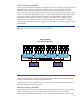

15
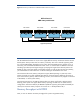
System memory bandwidth
By removing the front side bus and moving the memory controllers onto the processors, the newer
system architectures eliminate some of the previous memory bottlenecks. The maximum theoretical
memory bandwidth is unattainable in practice, because it represents an idealized scenario in which
all memory channels operate at full throughput all the time. Using NUMA architectures, 2P ProLiant
servers can achieve improved measured memory throughput relative to their theoretical maximums.
See Table 6 for details.
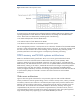
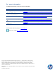
Table 6: Theoretical maximum versus measured memory throughput for 2P ProLiant servers
Theoretical maximum
memory bandwidth
Measured maximum memory
throughput
Intel-based 2P ProLiant G5 25.6 GB/s (RDIMMs)
38.4 GB/s (FBDIMMs)
12 GB/s
Intel-based 2P ProLiant G6/G7 64 GB/s 40 GB/s
Intel-based 2P ProLiant
Gen8
102.4 GB/s 88.6 GB/s
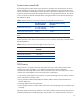
NUMA architecture also allows the 4P ProLiant G7 servers to deliver significantly increased memory
bandwidth (Table 7).
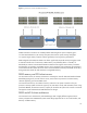
Table 7: Theoretical maximum memory throughput for 4P ProLiant servers
Theoretical maximum memory
bandwidth
Intel-based 4P ProLiant G5 38.4 GB/s (FBDIMMs)
Intel-based 4P ProLiant G7 136.4 GB/s
AMD-based 4P ProLiant G6 51.2 GB/s
AMD-based 4P ProLiant G7 169.6 GB/s
DDR3 latency
Memory latency is a measure of the time required for the CPU to receive data from the memory
controller once it has requested it. It is an important measurement of memory subsystem
responsiveness. Retrieving data from the memory subsystem consists of several steps, each of which
consumes time. Taken together, these times comprise the overall latency:
• Time memory request spends in the processor I/O queue and being sent to the memory controller
• Time in the memory controller queue
• Issuing of the Row Address Select (RAS) and Column Address Select (CAS) commands on the
memory address bus
• Retrieving data from the memory data bus
• Time through the memory controller and I/O bus back to the requesting processor Arithmetic Logic
Unit (ALU)
The setting of RAS and CAS lines determine which memory address will be accessed. The electrical
properties of DRAM are such that setting them requires about 13.5 nanoseconds each. This time is