
DDR3 memory technology

7
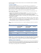
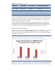
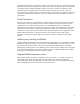
SmartMemory DIMMs support extended performance when compared to third party memory. This is
true for several DIMM types and configurations. Table 5 summarizes these performance extensions.
Table 5: Extended performance for HP SmartMemory DDR3 DIMMs in 2P ProLiant Gen8 servers
1 or 2 DIMMs per channel 3 DIMMs per channel
1600 MT/s
RDIMMs
1600 @ 1.5V 1333 @ 1.5V (HP SmartMemory and
RBSU option)
1066 @ 1.5V (3
rd
1333 MT/s
RDIMMs
Party)
1333 @ 1.35V (HP SmartMemory)
1333 @ 1.5V (3
rd
1066 @ 1.35V (HP SmartMemory)
1066 @ 1.5V (3 Party)
rd
1333 MT/s
LRDIMMS
Party)
1333 @ 1.35V (HP SmartMemory)
1333 @ 1.5V (3
rd
1066 @ 1.35V (HP SmartMemory)
1066 @ 1.5V (3 Party)
rd
Party)
1333 MT/s
UDIMMs
1333 MT/s (HP SmartMemory)
1066 MT/s (3
rd
Not Supported
Party)
The HP DDR3 Memory Configuration Tool provides additional assistance with configuring DDR3
memory (including HP SmartMemory) in HP ProLiant servers. It is available at
Core DDR3 Technologies
http://h18004.www1.hp.com/products/servers/options/tool/hp_memtool.html
DDR3 memory specifies data transfer rates that are greater than twice that of DDR2 memory.
Achieving these rates required significant engineering work to improve electrical signal integrity as
well as new technologies to address the increasingly small timing tolerances. DDR3 memory has also
added features to improve overall reliability and manageability.
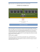
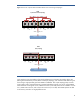
Fly-by topology
Fly-by topology is one of the key technological innovations that allow DDR3 DIMMs to achieve twice
the speed of DDR2 memory. In general, it refers to how address and command lines run to the
DRAMs on the DIMM module and the timing adjustments required on the memory controller to
compensate for it. To understand the workings of Fly-by topology, we will compare it to the T-Branch
topology used in DDR2.
Figure 3 shows how one of the address and command signals run to the DRAMs in an Unbuffered
DDR2 DIMM compared to a DDR3 DIMM. The symmetrical T-branch topology of DDR2 ensures that
command and address signals arrive at all the DRAMs as close to simultaneously as possible. With
this design, all of the DRAMs present their data (during a read) to the memory bus at the same time.
The memory controller then reads the set of parallel bits. The window of time when the data bits can
be read is known as the data eye, and the size of the eye shrinks as memory clock speeds increase.