
HP BladeSystem c-Class architecture Technology brief, 4th edition

12
High bandwidth and performance
BladeSystem c-Class enclosure capabilities allow you to change your configuration as the demand for
power and bandwidth grows:
• Blade form factors enable server-class components (discussed in the “
General-purpose flexible
design” section)
• High-bandwidth NonStop signal midplane
• Separate power backplane
NonStop signal midplane scalability
The NonStop signal midplane supports signal rates of up to 10 gigabits per second (Gb/s) per lane
(each lane consists of four SerDes transmit/receive traces). Each half-height server bay has 16 lanes
delivering the cross-sectional bandwidth to conduct up to 160 Gb/s per direction.
In a BladeSystem c7000 enclosure, the aggregate bandwidth between device bays and interconnect
bays is up to 5 terabits per second (Tb/s) across the NonStop signal midplane. Calculate the
aggregate backplane bandwidth as follows: 160 Gb/s x 16 device bays x 2 directions = 5.12Tb/s.
It is bandwidth between the device bays and interconnect bays. It does not include additional traffic
capacity between interconnect modules or cross-bay connections. Current half-height blades use 12 of
the 16 lanes to the interconnect bays.
One of the areas our engineering teams focused on was high-speed signal integrity. Getting this level
of bandwidth between bays required special attention to high-speed signal integrity:
• Using general best practices for signal integrity to minimize end-to-end signal losses across the
signal midplane
• Moving the power into an entirely separate backplane to independently optimize the NonStop
signal midplane
• Providing a method to set optimal signal waveform shapes in the transmitters, depending on the
topology of the end-to-end signal channel
Best practices
To ensure high-speed connectivity among all blades and interconnect modules, we leveraged our
many years of experience in designing HP Superdome computers. Specifically, our engineers paid
special attention to
• Controlling the differential signal impedance along each end-to-end signal trace across the PCBs
and through the connector stages
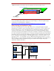
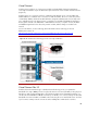
• Using a ground plane to isolate, receive, and transmit signal pins (see Figure 10)
• Keeping signal traces short to minimize losses
• Routing signals in groups to minimize signal skew