
HP Integrity rx7620 Server - User Service Guide, Sixth Edition

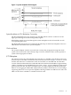
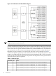

Figure 1-3 System Backplane Block Diagram
System Backplane to PCI-X Backplane Connectivity
The PCI-X backplane uses two connectors for the SBA link bus and two connectors for the
high-speed data signals and the manageability signals.
SBA link bus signals are routed through the system backplane to the cell controller on each
corresponding cell board.
The high-speed data signals are routed from the SBA chips on the PCI-X backplane to the two
LBA PCI bus controllers on the system backplane.
Clocks and Reset
The system backplane contains reset and clock circuitry that propagates through the whole
system. The central clocks drive all major chip set clocks. Therefore, these circuits represent a
system-wide single-point of failure.
I/O Subsystem
The cell board to the PCI-X board path runs from the CC to the SBA, from the SBA to the ropes,
from the ropes to the LBA, and from the LBA to the PCI slots seen in Figure 1-4. The CC on cell
board 0 and cell board 1 communicates with one each SBA over the SBA link. The SBA link
consists of both an inbound and an outbound link with an effective bandwidth of approximately
1 GB/sec. The SBA converts the SBA link protocol into “ropes.” A rope is defined as a high-speed
point-to-point data bus. The SBA can support up to 16 of these high-speed bi-directional rope
links for a total aggregate bandwidth of approximately 4 GB/sec. Each LBA acts as a bus bridge,
supporting either one or two ropes and capable of driving 33 Mhz or 66 Mhz for PCI cards. The
LBAs can also drive at 66 Mhz or 133 Mhz for PCI-X cards.
Overview 19