
ISS Technology Update, Volume 9, Number 2

3
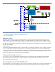
Figure 1-2. FBWC cache module block diagram
FPGA
RoC
NAND Flash NAND Flash
PROM
DRAM
8X
DRAM
8X
DRAM
8X
System board
Cache module
System board
Cache module
133 MHZ DDR IF
Register
TWI**
Reg reset N
Reset N
Cache dirty N*
Command
& address
Data
400 MHZ DDR IF
Side band
control
signals
Super-cap
In off-module pack connecting to
cache module
4b 33MHz4b 33MHz
4b 33MHz4b 33MHz
* Cache tracks that have been written over are designated as "dirty"
** Two wire interface (TWI)
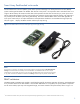
FBWC cache module
The FBWC cache module has a field programmable gate array (FPGA), DDR2 DRAMs, and NAND flash devices. The
module supports up to 1GiB of DDR2 memory and up to 72 data bits (64 data bits plus 8 ECC bits). The FBWC module
connects to the Smart Array controller through a 244-pin mini-DIMM connector. When the Smart Array controller is driving
the DDR2 bus, data rates of up to 800Mbps are supported. When the FPGA is driving the bus in a data recovery situation,
the data rate is 266Mbps.
Super-capacitor
T
he Super-cap module sub-assembly consists of two 35-Farad, 2.7-V capacitors configured in series, providing 17 Farads at
up to 5.4 V. The charger maintains the Super-cap at 4.8 V, providing the required amount of power to complete backup
operations while extending the life of the Super-cap. The charger also monitors Super-cap health and activates LED indicators
on the FBWC module to warn of impending failure. The Super-cap module is contained within the same form factor and
housing as the HP-650 mAh P-Series battery used in the HP BBWC.
Capturing data during power loss
Loss of power in a server using the FBWC prompts the FPGA to copy data contained in the DRAM to the NAND flash
devices residing on the cache module. The Super-cap supplies the energy needed to power the FBWC system while
performing the data backup operation.
Recovering data from the flash-backed cache
When system power is present, the FPGA is in its idle state. In the idle state, the FPGA simply monitors the voltage status, the
resets, and the control signals managed by the Smart Array controller. The FPGA DDR2 I/O pins are held in “tri-state,”