
Memory technology evolution: an overview of system memory technologies, 9th edition

DRAM storage density and power consumption
DRAM storage capacity is inversely proportional to the cell geometry. In other words, the storage density
increases as the cell geometry shrinks. Over the past few years, capacity has expanded from 1 kilobit (Kb)
per chip to 2 gigabit (Gb) per chip. We expect that the capacity will soon grow to 4 Gb per chip.
The industry-standard operating voltage for computer memory components was originally 5 volts. But as cell
geometries decreased, memory circuitry became smaller and more sensitive. Likewise, the industry-standard
operating voltage decreased. Today, computer memory components operate at 1.8 volts, letting them run
faster and consume less power.
Memory access time
The elapsed time from the assertion of the CAS signal until the data is available on the data bus is the
memory access time or CAS latency. For asynchronous DRAM, we measure memory access time in
nanoseconds. For synchronous DRAM, we measure memory access time by the number of memory bus
clocks.
System bus timing
A system bus clock controls all computer components that execute instructions or transfer data. The system
chipset controls the speed, or frequency, of the system bus clock. The system chipset also regulates the
traffic between the processor, main memory, PCI bus, and other peripheral buses.
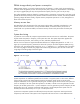
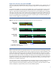
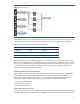
The bus clock is an electronic signal that alternates between two voltages (designated as “0” and “1” in
Figure 3) at a specific frequency, measured in millions of cycles per second or megahertz (MHz). During
each clock cycle, the voltage signal moves from "0" to "1" and back to "0.” A complete clock cycle spans
from one rising edge to the next rising edge. Data transfer along the memory bus can start on either the
rising edge or the falling edge of the clock signal.
Figure 3. A bus clock signal
System components run at different speeds from one another in a typical system. For this reason, different
clocks running at various but related speeds control the components. These clocks use various clock
multiplier and divider circuits to generate multiple signals. All these signals derive from the main system bus
clock. For example, if the main system bus operates at 100 MHz, a divider circuit can generate a PCI bus
frequency of 33 MHz (system clock ÷ 3) and a multiplier circuit can generate a processor frequency of 400
MHz (system clock x 4). Computer components that operate in whole multiples of the system clock are
termed synchronous because they are “in sync” with the system clock.
Synchronous components operate more efficiently than asynchronous components. With asynchronous
components, either the rest of the system or the component itself must wait one or more additional clock
4