
Double Data Rate SDRAM: Fast Performance at an Economical Price

Double Data Rate SDRAM: Fast
TECHNOLOGY BRIEF (cont.) Performance at an Economical Price
3
Doc Number TC020603TB
.
.
.
.
.
.
.
.
.
.
.
.
.
.
.
.
.
.
.
.
.
.
.
.
.
.
.
.
.
.
.
.
.
.
.
.
.
.
.
.
.
.
.
.
.
.
.
.
.
.
.
.
.
.
.
.
.
.
.
.
.
.
.
.
.
.
.
.
.
.
.
.
.
.
.
.
.
.
.
.
.
.
.
.
.
.
.
.
.
.
.
.
.
.
.
.
.
.
.
.
.
.
.
.
.
.
.
.
.
.
.
.
.
.
.
.
.
.
.
.
.
.
.
.
.
.
.
.
.
.
.
.
.
.
.
.
.
.
.
.
.
.
.
.
.
.
.
.
.
.
.
.
.
.
.
.
.
.
.
.
.
INTRODUCTION
Double Data Rate SDRAM has been around for awhile, but it has been in a battle for its very
survival. At first, it was thought that DDR SDRAM would simply prolong the life of SDRAM
technology until a revolutionary memory technology came to market. DDR SDRAM has not only
survived, but it is becoming more widely accepted. DDR SDRAM delivers twice the bandwidth of
SDRAM, yet DDR SDRAM has the same core design as regular SDRAM. Therefore, it has been
easier and cheaper for memory manufacturers to convert production lines to DDR than to retool to
adopt a revolutionary memory technology like Rambus DRAM. These factors translate into much
faster performance from DDR SDRAM at a lower cost.
The JEDEC Solid State Technology Association, the semiconductor engineering standardization
body of the Electronic Industries Alliance, is currently developing the next-generation DDR
SDRAM technology, called DDR SDRAM II.
This paper begins with a description of synchronous DRAM operation because it is a prerequisite
to understanding the evolution of DDR SDRAM. Readers already familiar with SDRAM may
choose to skip forward to the section entitled “Double Data Rate SDRAM.”
SDRAM OPERATION
Computers use two types of system memory—cache memory and main memory. Cache memory
consists of very fast static RAM chips. The most prevalent type of main memory used today is
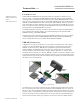
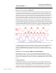
SDRAM. As shown in Figure 1, SDRAM chips are installed on 168-pin dual inline memory
modules (DIMMs). Each SDRAM chip consists of an array (columns and rows) of capacitors,
which act as memory cells that store data. A charged capacitor represents a “1” data bit, and an
uncharged capacitor represents a “0” data bit. SDRAM is “dynamic” because the capacitors need to
be recharged (refreshed) by electric pulses thousands of times per second to retain the data. On the
periphery of the array of memory cells are transistors that read, amplify, and transfer the data from
the memory cells to the memory bus.
Figure 1. Main Memory
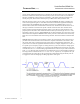
The memory bus is a circuit that consists of two parts: the data bus and the address bus. The data
bus is a set of lines (traces) that carry the actual data to and from SDRAM. Each trace carries one
data bit at a time. The throughput (bandwidth) of the data bus depends on its width (in bits) and its
frequency. Today’s computers have a 64-bit wide data bus, which means that the bus transports 64
bits (one data word) at a time. The address bus is a set of traces that carry signals identifying the
location of data in memory and the type of memory access (read or write). The address bus also
SDRAM: synchronous
dynamic random access
memory
D
DR: double data rate