
Double Data Rate SDRAM: Fast Performance at an Economical Price

Double Data Rate SDRAM: Fast
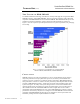
TECHNOLOGY BRIEF (cont.) Performance at an Economical Price
4
Doc Number TC020603TB
.
.
.
.
.
.
.
.
.
.
.
.
.
.
.
.
.
.
.
.
.
.
.
.
.
.
.
.
.
.
.
.
.
.
.
.
.
.
.
.
.
.
.
.
.
.
.
.
.
.
.
.
.
.
.
.
.
.
.
.
.
.
.
.
.
.
.
.
.
.
.
.
.
.
.
.
.
.
.
.
.
.
.
.
.
.
.
.
.
.
.
.
.
.
.
.
.
.
.
.
.
.
.
.
.
.
.
.
.
.
.
.
.
.
.
.
.
.
.
.
.
.
.
.
.
.
.
.
.
.
.
.
.
.
.
.
.
.
.
.
.
.
.
.
.
.
.
.
.
.
.
.
.
.
.
.
.
.
.
.
.
carries control signals that enable devices to negotiate for use of the memory bus. The width of the
address bus controls how much system memory the processor can read or write to; but unlike the
data bus, its width has no direct impact on performance. The memory subsystem operates at the
memory bus speed, which has the same frequency (in MHz) as the main system bus clock.
When the processor needs to access (read or write) data in SDRAM, the memory controller first
sends control signals that gain use of the data bus and then sends address signals that identify the
location of the data in SDRAM. When the address signals arrive at SDRAM, they go to a row
address selector (RAS) and a column address selector (CAS). The RAS activates the entire row of
the target cell and the CAS selects the specific cell that contains the data. The controller sends
another signal to designate whether data will be written or read. By way of the transistors on the
periphery of the cells, data is then transferred from the memory bus to the target cell or vice versa,
depending on the type of access. While SDRAM cells are being refreshed, they cannot be accessed
until the refresh is completed. SDRAM divides memory into two to four banks so that one memory
bank can be accessed while the other bank is being refreshed. This division allows continuous data
flow.
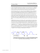
SDRAM differs from earlier types of memory in that it runs synchronously to the system clock. If
you think of the numerous devices and circuits in the computer as musicians in an orchestra, then
the system clock is like a conductor that keeps perfect time to coordinate their performance. The
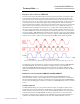
system clock is an electronic signal that alternates between two voltages, designated as “0” and “1”,
at a specific pace or frequency (Figure 1). During each tick (cycle) of the clock, the voltage signal
transitions from "0" to "1" and back to "0". The rising edge marks the start of the clock cycle when
it transitions from “0” to “1 and the falling edge marks the end of the clock cycle when it transitions
from “1” to “0”. Because these transitions are not instantaneous, the rise time and fall time measure
how long it takes to transition from “0” to “1” and “1” to “0”, respectively. A complete clock cycle
is measured from one rising edge to the next rising edge. Data transfer along the memory bus can
be triggered on either the rising edge or falling edge of the clock signal.
Figure 2. Representation of a bus clock signal