
Double Data Rate SDRAM: Fast Performance at an Economical Price

Double Data Rate SDRAM: Fast
TECHNOLOGY BRIEF (cont.) Performance at an Economical Price
5
Doc Number TC020603TB
.
.
.
.
.
.
.
.
.
.
.
.
.
.
.
.
.
.
.
.
.
.
.
.
.
.
.
.
.
.
.
.
.
.
.
.
.
.
.
.
.
.
.
.
.
.
.
.
.
.
.
.
.
.
.
.
.
.
.
.
.
.
.
.
.
.
.
.
.
.
.
.
.
.
.
.
.
.
.
.
.
.
.
.
.
.
.
.
.
.
.
.
.
.
.
.
.
.
.
.
.
.
.
.
.
.
.
.
.
.
.
.
.
.
.
.
.
.
.
.
.
.
.
.
.
.
.
.
.
.
.
.
.
.
.
.
.
.
.
.
.
.
.
.
.
.
.
.
.
.
.
.
.
.
.
.
.
.
.
.
.
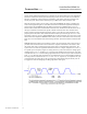
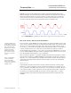
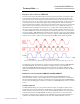
SDRAM uses a process called data bursting to achieve greater data throughput than previous
DRAM technologies. The initial data word is usually transferred on the sixth clock cycle after the
request is received (see Figure 3). Using burst mode access, data is burst out (or in) with every
clock cycle after the first access. After the memory controller sends the initial CAS, up to four
consecutive 64-bit data words can be accessed before it has to send another CAS.
Figure 3. Burst mode access of SDRAM (top). Data transfer is triggered on the rising edge of the clock.
How CAS Latency Affects System Performance
Now let's review a typical SDRAM access using a memory bus speed of 100 MHz (10 ns per clock
cycle). First, the controller activates the row and bank using the RAS signal. After a period of time,
the target cell is selected with the CAS signal. Then it takes a period of time, called the column
access time (t
CAC
), for the data to be transported to the output transistor where it can be transferred
to the bus on the next clock cycle. At this point, the time needed for the first piece of data to
become available is the CAS latency—2 or 3 clock cycles for unbuffered DIMMs and 3 or 4 clock
cycles for buffered DIMMs. Subsequent transfers are performed in burst mode (every clock cycle)
up to the programmed burst length of 1, 2, 4, or 8 data words.
Why is CAS latency important? To guarantee compliance with the PC100 specification, vendors
must specify the CAS latency of SDRAM DIMMs. The specification only allows for CAS latency
values of 1, 2, or 3. The CAS latency (CL) is based on the column access time, the time it takes to
transfer data to the output transistors from the time the CAS line is activated. CL is determined
using the equation:
CL * t
CLK
>= t
CAC
In plain English, this means that the time it can take to transfer data from the cell to the output
transistor (t
CAC
) has to be less than one clock cycle times the CAS latency. For example, if t
CLK
is
10 ns (cycle time for a 100-MHz system clock) and t
CAC
is 20 ns, then the CL must be 2. But if t
CAC
is 25 ns, then CL must be 3. Some vendors refer to these values as CAS2 and CAS3, respectively.
For memory to be certified at 100 MHz, the CAS latency cannot be higher than 3. A CAS2 is
slightly faster than a CAS3, which theoretically makes it function better in systems faster than
100 MHz.
Unbuffered DIMMs do not
use any buffer logic chips.
B
y eliminating propagation
delay of the logic buffer
during the first read/write
operation, unbuffered
D
IMMs achieve slightly
f
aster operation (by one
clock cycle at the initial
access
)
.
P
C100: a DIMM that is
rated at 8 ns and has
other internal timing
characteristics that allow
it to function properly in a
100 MHz system.