
Double Data Rate SDRAM: Fast Performance at an Economical Price

Double Data Rate SDRAM: Fast
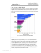
TECHNOLOGY BRIEF (cont.) Performance at an Economical Price
6
Doc Number TC020603TB
.
.
.
.
.
.
.
.
.
.
.
.
.
.
.
.
.
.
.
.
.
.
.
.
.
.
.
.
.
.
.
.
.
.
.
.
.
.
.
.
.
.
.
.
.
.
.
.
.
.
.
.
.
.
.
.
.
.
.
.
.
.
.
.
.
.
.
.
.
.
.
.
.
.
.
.
.
.
.
.
.
.
.
.
.
.
.
.
.
.
.
.
.
.
.
.
.
.
.
.
.
.
.
.
.
.
.
.
.
.
.
.
.
.
.
.
.
.
.
.
.
.
.
.
.
.
.
.
.
.
.
.
.
.
.
.
.
.
.
.
.
.
.
.
.
.
.
.
.
.
.
.
.
.
.
.
.
.
.
.
.
DOUBLE DATA R ATE SDRAM
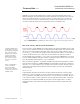
Processors today operate much faster than the memory subsystem; therefore, increasing the speed
of the memory bus would improve overall system performance more than further increasing the
speed of the processor. System designers can speed up the memory bus by increasing the system
clock frequency; however, this creates several issues regarding signal integrity. As the system clock
frequency increases, the timing becomes tighter. Tighter timing increases both the interference
between signals and the hardware costs because circuits must be made more precise to deal with the
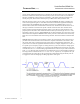
higher speeds. So system designers came up with an innovative way to double the memory bus
bandwidth without increasing the clock frequency—by using both the rising and falling edges of
the clock to trigger data transfer. This technology, known as double transition clocking, is not new.
Accelerated Graphics Port (AGP) technology uses it to double I/O performance over conventional
PCI buses. Similarly, DDR SDRAM uses double transition clocking to deliver twice the bandwidth
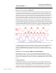
of standard DRAM without increasing the clock frequency (Figure 4). DDR SDRAM has peak data
transfer rates of 1.6 and 2.1 GB/s at clock frequencies of 100 MHz and 133 MHz, respectively.
Figure 4. Representation of DDR SDRAM transferring data on the rising and falling edges of the clock.
The following section will summarize at a high level the basic differences between DDR SDRAM
and standard SDRAM. This section will clarify the challenges faced by system designers in
implementing DDR SDRAM and describe the technical advances and physical differences that
make it incompatible with standard SDRAM. The subsequent section will describe plans for DDR
SDRAM II.
Differences between Standard SDRAM and DDR SDRAM
DDR SDRAM has the same core design as standard SDRAM, but DDR SDRAM has some
enhancements that enable it to achieve higher data rates: 2n-Prefetch Architecture, a strobe-based
data bus, different signaling technology, and reduced power requirements. Because DDR SDRAM
uses the rising and falling edges of the clock, CAS latency for DDR SDRAM is 2 and 2.5 instead of
2 and 3.
2n-Prefetch Architecture
The DDR SDRAM design uses a 2n-prefetch architecture, which, at a high level, means that its
internal data bus is twice the width of the external data bus. This means that a single read access
fetches two data words instead of just one as with standard SDRAM. Similarly, two data words are
combined and written to the DDR SDRAM core during a single write access. A more detailed
description is outside the scope of this paper. More information on the 2n-prefetch architecture is
available in the JEDEC standard JESD79, Double Data Rate (DDR) SDRAM Specification.