
Double Data Rate SDRAM: Fast Performance at an Economical Price

Double Data Rate SDRAM: Fast
TECHNOLOGY BRIEF (cont.) Performance at an Economical Price
7
Doc Number TC020603TB
.
.
.
.
.
.
.
.
.
.
.
.
.
.
.
.
.
.
.
.
.
.
.
.
.
.
.
.
.
.
.
.
.
.
.
.
.
.
.
.
.
.
.
.
.
.
.
.
.
.
.
.
.
.
.
.
.
.
.
.
.
.
.
.
.
.
.
.
.
.
.
.
.
.
.
.
.
.
.
.
.
.
.
.
.
.
.
.
.
.
.
.
.
.
.
.
.
.
.
.
.
.
.
.
.
.
.
.
.
.
.
.
.
.
.
.
.
.
.
.
.
.
.
.
.
.
.
.
.
.
.
.
.
.
.
.
.
.
.
.
.
.
.
.
.
.
.
.
.
.
.
.
.
.
.
.
.
.
.
.
.
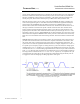
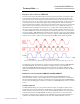
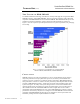
Strobe-based Data Bus
In a synchronous system, data output and capture are referenced to transitions in the system clock.
When the clock signal transitions, an operation is signaled to begin; however, a period of time must
pass before the signal stabilizes. As shown in Figure 5, access time (t
AC
) is the amount of time it
takes to "open" the output line from the prior clock "tick.” t
AC
is specified as a maximum value
because one DDR DRAM chip may have a t
AC
=4 ns while another chip may have a t
AC
=6 ns. To be
able to send data out on every clock cycle, t
AC
must be fast enough to allow the signal to stabilize
before beginning the actual output operation.
Figure 5. Representation of the data valid window, or data eye, for DDR SDRAM.
Because of possible distortion (skew) in the SDRAM chips and printed circuit board, as the bus
frequency increases, it can become more difficult for components to capture data using a clock.
This is especially true for DDR SDRAM because its data capture rate is twice the clock frequency.
The issue is that the region where the data is valid (called a data eye) is so small that it is very
difficult to meet setup and hold timing (the period of time that must pass to allow the signal to
stabilize). For example, if the bus frequency is increased to 200 MHz, the clock cycle (transition) is
only 5 ns. In an ideal world, each data word (64 bits) sent by the source device would arrive at the
capturing device at exactly the same time so they could be captured every 5 ns. However, because
of real factors such as trace length differences and variations in temperature, voltage, and
manufacturing processes, the data eye may move in relation to the fixed clock signal. As a result,
the time the data is stable is 5 ns minus the extra delays.
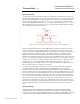
To assist with the tight timing requirements, the source device sends a reference signal called a
strobe with the data. The data strobe signal helps the capturing device to locate data more
accurately and resynchronize incoming data from different DIMMs. During a write operation, the
memory controller places the rising and falling edge of the strobe in the middle of the data eye so it
can be used to capture the data at the SDRAM. For read accesses, SDRAM also sends data with a
strobe, but the strobe edge is aligned with the data. The device receiving the read data must shift
the strobe to the center of the data eye. Read and write accesses have different strobe alignment so
that the delay circuitry can be centralized in one place (the controller) and does not have to be
replicated in every DRAM device in the system. Although tight system timing requirements were
alleviated on the data bus by using bi-directional strobes, they were not removed for the command
bus. The command bus does not use a strobe and must still meet setup times to a synchronous
clock.
Signaling Technology
Another difference between SDRAM and DDR SDRAM is the signaling technology. DDR
SDRAM uses Stub Series Terminated Logic (SSTL) instead of the Low Voltage Transistor-to-
Transistor Logic (LVTTL) that standard SDRAM uses. This signaling interface change, in addition
to using data strobes, allows DDR SDRAM to run at faster speeds than traditional SDRAM.