
Technologies for the ProLiant ML570 G3 and ProLiant DL580 G3 Servers Technology Brief
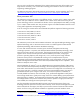


Intel E8500 chipset
The E8500 chipset has a high-availability memory subsystem that consists of the North Bridge (TNB)
and the XMB memory controller.
The E8500 chipset is designed to support the upcoming dual-core versions of Intel processors, and
has the important feature of using two separate front side buses to connect to the processors
(Figure 2). Each north bridge can connect to up to four memory boards, and each memory board
includes an XMB memory controller chip. The north bridge connects to each XMB memory controller
using a high-speed serial interconnect (the IMI bus) that allows 5.3 GB/s inbound (for read data
signals from the XMB) and 2.7 GB/s outbound (for write data signals to the XMB). This inbound
speed matches the throughput of the front-side buses, providing a good balance between the
processor and memory subsystem. The north bridge uses an in-order (FIFO) queue to maintain
coherency across the dual front-side buses while processing read/write requests.
Figure 2. Xeon MP architecture used in the ProLiant ML570 G3 and DL580 G3 platforms
Each XMB memory controller chip supports two channels of DDR-2 memory. The DDR-2 memory on
each channel operates in lockstep at 400 MHz. The ProLiant ML570 G3 supports 6 DIMMs per
memory board (three per channel), and the ProLiant DL580 supports 4 DIMMs per memory board
(two per channel), due to physical constraints of the 4U system. For both servers, the maximum
memory supported is 64 GB with 4-GB DIMMs, as described in the section “Maximum memory
configurations.”
6