
HP Smart Array Controller technology, 4th edition

11
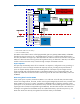
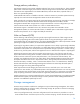
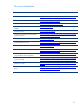
Figure 1. FBWC block diagram
FPGA
RoC
NAND Flash NAND Flash
PROM
DRAM
8X
DRAM
8X
DRAM
8X
System board
Cache module
System board
Cache module
133 MHZ DDR IF
Register
TWI**
Reg reset N
Reset N
Cache dirty N*
Command
& address
Data
400 MHZ DDR IF
Side band
control
signals
Super-cap
In off-module pack connecting to
cache module
4b 33MHz4b 33MHz
4b 33MHz4b 33MHz
* Cache tracks written over are “dirty."
** Two-wire interface (TWI)
The FBWC cache module contains a field programmable gate array (FPGA), DDR2 DRAMs, and NAND
flash devices that can support up to 1 GB of DDR2 memory and up to 72 data bits (64 data bits plus 8
ECC bits). The FBWC can support up to 800 Mb/s data rate when the Smart Array controller is driving the
DDR2 bus. When the FPGA is driving the bus during data recovery, the data rate is 266 Mb/s. The FBWC
module connects to the Smart Array controller through a 244-pin mini-DIMM connector.
Super-capacitor
T
he Super-cap sub-assembly consists of two 35-Farad 2.7V capacitors, configured in series, providing 17
Farads at up to 5.4V. The charger maintains the Super-cap at 4.8V, providing the required amount of
power to complete backup operations while extending the life of the Super-cap. The charger monitors
Super-cap health and activates LED indicators on the FBWC module to warn of impending failure. The
Super-Cap module uses the same form factor and housing as the HP 650 mAh P-Series battery used in the
HP BBWC.
Recovering data from the FBWC
When syst
em power is present, the FPGA on FBWC is in its idle state. In the idle state, the FPGA simply
monitors the voltage statuses, the resets, and the control signals managed by the Smart Array controller. The
FPGA’s DDR2 I/O pins are in “tri-state,” equivalent to a disabled mode, to avoid bus contention. When
system power is lost, the FPGA waits for the Smart Array controller’s clock enable signal to transition to low,
signaling that the controller has stopped driving the DDR2 bus. The FPGA then assumes control of the bus
and begins moving data from the DRAMs to the non-volatile flash memory. Upon the next power up, the
FPGA then restores the cache by moving data from the flash memory to the DRAMs.