
Solid State Drive Technology Differences between SLC, MLC and TLC NAND
Technical white paper | Solid State Drive Technology
2
Executive summary
This document outlines the differences between three different NAND technologies: SLC, MLC, and TLC.
• SLC - Single level cell provides high performance, low power consumption; faster write speeds, and higher program/erase
cycles per cell, but at a higher cost. These devices are mainly used in high end server applications.
• MLC - Multi level cell provides a lower cost than SLC; however, MLC has a lower endurance limit and lower program/erase
cycles than SLC, and is a good fit for commercial/workstations platforms and applications.
• TLC - Three level cell provides higher density, but has lower endurance limits, slower write read speeds, and lower
program/erase cycles than SLC and MLC. To this point, TLC NAND has been used primarily in flash devices; however,
technological advancements are making TLC an option for normal applications.
SLC vs MLC vs TLC
NAND cell technology
A single NAND flash die is typically subdivided into 512 MB blocks, and each block is typically subdivided into 4 KB pages. You
can read and write to individual pages as long as they are empty; however, once a page is written, it can’t be overwritten - it
must be erased first before it can be written to again. This sequence of writing, erasing, and then writing again is known as
the Program/Erase cycle. The P/E cycle can serve as a criterion for quantifying the endurance of a flash storage device.
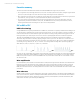
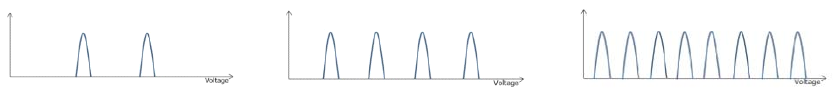
Physically, all three NAND technologies consist of similar transistors; the only difference is that they store different
amounts of charge. All three work similarily, applying voltage to a cell to go from an “off” state to an “on” state. SLC uses
two distinct voltage states representing one bit per cell and two logic levels (0 and 1). MLC uses four distinct voltage states
representing four logic states (00, 01, 10, 11) or two bits. TLC uses eight distinct voltage states representing eight logic
states (000, 001, 010, 011, 100, 101, 110, and 111), or three bits.
SLC MLC TLC
Since SLC uses two voltage states, these states can be further apart, reducing the potential to incorrectly interpret the state
of the cell and allowing for standard NAND error conditions, like read disturbs. The possibility for errors increases with TLC
NAND, so it requires more ECC correction as the NAND wears out, because there are three bits to correct instead of one for
SLC and two for MLC.
Write amplification
In write amplification, the actual amount of data written is a multiple of the logical amount intended to be written. Because
flash memory must be erased before it can be rewritten, the process to perform these operations results in moving user
data and metadata more than once. This multiplying effect increases the number of writes required over the life of the
NAND, which shortens the time it can reliably operate. This increase in write consumes bandwidth and reduces random write
performance.
Write endurance
All SSDs specify an endurance number that relates to the number of Program/Erase cycles that the underlying NAND array
can accept. This endurance, defined in Total Bytes Written (TBW), specifies the number of host writes that can be written to
the drive. In this endurance number, SSD vendors assume a workload, write amplification, and wear level efficiency that
determine the actual P/E cycles allowed by the NAND array.