Technical Reference Guide HP Compaq dc7800 Series Business Desktop Computers Document Part Number: 461444-001 October 2007 This document provides information on the design, architecture, function, and capabilities of the HP Compaq dc7800 Series Business Desktop Computers. This information may be used by engineers, technicians, administrators, or anyone needing detailed information on the products covered.
© Copyright 2007 Hewlett-Packard Development Company, L.P. The information contained herein is subject to change without notice. Microsoft, MS-DOS, Windows, and Windows NT are trademarks of Microsoft Corporation in the U.S. and other countries. Intel, Intel Core 2 Duo, Intel Core 2 Quad, Pentium Dual-Core, Intel Inside, and Celeron are trademarks of Intel Corporation in the U.S. and other countries. Adobe, Acrobat, and Acrobat Reader are trademarks or registered trademarks of Adobe Systems Incorporated.
Contents 1 Introduction 1.1 About this Guide . . . . . . . . . . . . . . . . . . . . . . . . . . . . . . . . . . . . . . . . . . . . . . . . . . . . . . . . . . . . . 1.1.1 Online Viewing . . . . . . . . . . . . . . . . . . . . . . . . . . . . . . . . . . . . . . . . . . . . . . . . . . . . . . . . . 1.1.2 Hardcopy . . . . . . . . . . . . . . . . . . . . . . . . . . . . . . . . . . . . . . . . . . . . . . . . . . . . . . . . . . . . . . 1.2 Additional Information Sources . . . . . . . . . . . . . . . . . .
Contents 3 Processor/Memory Subsystem 3.1 Introduction . . . . . . . . . . . . . . . . . . . . . . . . . . . . . . . . . . . . . . . . . . . . . . . . . . . . . . . . . . . . . . . . . 3.2 Intel Processors . . . . . . . . . . . . . . . . . . . . . . . . . . . . . . . . . . . . . . . . . . . . . . . . . . . . . . . . . . . . . . 3.2.1 Intel Processor Overview . . . . . . . . . . . . . . . . . . . . . . . . . . . . . . . . . . . . . . . . . . . . . . . . . . 3.2.2 Processor Changing/Upgrading . . . . . . . .
Contents 5.7.3 Keyboard/Pointing Device Interface Connector . . . . . . . . . . . . . . . . . . . . . . . . . . . . . . . 5.8 Universal Serial Bus Interface. . . . . . . . . . . . . . . . . . . . . . . . . . . . . . . . . . . . . . . . . . . . . . . . . . 5.8.1 USB Connector. . . . . . . . . . . . . . . . . . . . . . . . . . . . . . . . . . . . . . . . . . . . . . . . . . . . . . . . . 5.8.2 USB Cable Data . . . . . . . . . . . . . . . . . . . . . . . . . . . . . . . . . . . . . . . . . . . . . . . . . . .
Contents 8 SYSTEM BIOS 8.1 Introduction . . . . . . . . . . . . . . . . . . . . . . . . . . . . . . . . . . . . . . . . . . . . . . . . . . . . . . . . . . . . . . . . . 8.2 ROM Flashing . . . . . . . . . . . . . . . . . . . . . . . . . . . . . . . . . . . . . . . . . . . . . . . . . . . . . . . . . . . . . . . 8.2.1 Upgrading . . . . . . . . . . . . . . . . . . . . . . . . . . . . . . . . . . . . . . . . . . . . . . . . . . . . . . . . . . . . . . 8.2.2 Changeable Splash Screen . . . . . . . . . . . . . .
1 Introduction 1.1 About this Guide This guide provides technical information about HP Compaq dc7800 Business PC personal computers that feature Intel processors and the Intel Q35 Express chipset. This document describes in detail the system's design and operation for programmers, engineers, technicians, and system administrators, as well as end-users wanting detailed information.
Introduction 1-2 www.hp.
Introduction 1.4 Serial Number The serial number is located on a sticker placed on the exterior cabinet. The serial number is also written into firmware and may be read with HP Diagnostics or Insight Manager utilities. 1.5 Notational Conventions The notational guidelines used in this guide are described in the following subsections. 1.5.
Introduction 1.6 Common Acronyms and Abbreviations Table 1-1 lists the acronyms and abbreviations used in this guide.
Introduction Table 1-1 (Continued) Acronyms and Abbreviations Acronym or Abbreviation Description Ch Channel, chapter cm centimeter CMC cache/memory controller CMOS complimentary metal-oxide semiconductor (configuration memory) Cntlr controller Cntrl control codec 1. coder/decoder 2. compressor/decompressor CPQ Compaq CPU central processing unit CRIMM Continuity (blank) RIMM CRT cathode ray tube CSM 1. Compaq system management 2.
Introduction Table 1-1 (Continued) Acronyms and Abbreviations 1-6 Acronym or Abbreviation Description ESCD Extended System Configuration Data (format) EV Environmental Variable (data) ExCA Exchangeable Card Architecture FIFO first in/first out FL flag (register) FM frequency modulation FPM fast page mode (RAM type) FPU Floating point unit (numeric or math coprocessor) FPS Frames per second ft Foot/feet GB gigabyte GMCH Graphics/memory controller hub GND ground GPIO general p
Introduction Table 1-1 (Continued) Acronyms and Abbreviations Acronym or Abbreviation Description Kb/KB kilobits/kilobytes (x 1024 bits/x 1024 bytes) Kb/s kilobits per second kg kilogram KHz kilohertz kV kilovolt lb pound LAN local area network LCD liquid crystal display LED light-emitting diode LPC Low pin count LSI large scale integration LSb/LSB least significant bit/least significant byte LUN logical unit (SCSI) m Meter MCH Memory controller hub MMX multimedia extensio
Introduction Table 1-1 (Continued) Acronyms and Abbreviations 1-8 Acronym or Abbreviation Description PC Personal computer PCA Printed circuit assembly PCI peripheral component interconnect PCI-E PCI Express PCM pulse code modulation PCMCIA Personal Computer Memory Card International Association PEG PCI express graphics PFC Power factor correction PIN personal identification number PIO Programmed I/O PN Part number POST power-on self test PROM programmable read-only memory PT
Introduction Table 1-1 (Continued) Acronyms and Abbreviations Acronym or Abbreviation Description SGRAM Synchronous Graphics RAM SIMD Single instruction multiple data SIMM single in-line memory module SMART Self Monitor Analysis Report Technology SMI system management interrupt SMM system management mode SMRAM system management RAM SPD serial presence detect SPDIF Sony/Philips Digital Interface (IEC-958 specification) SPN Spare part number SPP standard parallel port SRAM static RA
Introduction Table 1-1 (Continued) Acronyms and Abbreviations 1-10 Acronym or Abbreviation Description VAC Volts alternating current VDC Volts direct current VESA Video Electronic Standards Association VGA video graphics adapter VLSI very large scale integration VRAM Video RAM W watt WOL Wake-On-LAN WRAM Windows RAM ZF zero flag ZIF zero insertion force (socket) www.hp.
2 System Overview 2.1 Introduction The HP Compaq dc7800 Business PC personal computers (Figure 2-1) deliver an outstanding combination of manageability, serviceability, and compatibility for enterprise environments. Based on the Intel processor with the Intel Q35 Express chipset, these systems emphasize performance along with industry compatibility. These models feature a similar architecture incorporating both PCI 2.3 and PCIe buses.
System Overview 2.2 Features The following standard features are included on all models unless otherwise indicated: 2-2 ■ Intel processor in LGA775 (Socket T) package ■ Integrated graphics controller ■ PC2-6400 and PC2-5300 (DDR2) DIMM support ■ Hard drive fault prediction ■ Eight USB 2.
System Overview Table 2-1 shows the differences in features between the different PC series based on form factor: Table 2-1 Feature Difference Matrix by Form Factor USDT SFF CMT 2 SODIMM 4GB 4 DIMM 8GB 4 DIMM 8GB Serial ports 0 1 std., 1 opt. [1] 1 std., 1 opt.
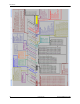
System Overview 2.3 System Architecture The systems covered in this guide feature an architecture based on the Intel Q35 Express chipset (Figure 2-13). All systems covered in this guide include the following key components: ■ Intel Pentium Dual-Core, Core 2 Duo, Core 2 Quad, or Celeron processor.
System Overview Intel Processor 800/1066/1333-MHz FSB Analog Monitor Digital Monitor [1] PCI Express x16 slot (PEG)[2] Q35 Chipset RGB DVI Integrated Graphics Q35 Cntlr. GMCH SDRAM Cntlr PCIe PEG I/F [2] DMI SATA Hard Drive SATA-to -PATA Bridge [1] Optical Drive AD1884 Audio Subsystem DMI SATA I/F 82801 ICH9 USB I/F Ch A DDR2 SDRAM Ch B DDR2 SDRAM USB Ports [5] Serial I/F [2] Parallel I/F [2] SCH5327 I/O Cntlr. LPC I/F Kybd-Mouse I/F Diskette I/F [2] Audio I/F PCI Cntlr. Keyboard PCI 2.
System Overview 2.3.
System Overview 2.3.2 Chipset The Intel Q35 Express chipset consists of a Graphics Memory Controller Hub (GMCH) and an enhanced I/O controller hub (ICH9-DO). Table 2-3 compares the functions provided by the chipsets.
System Overview 2.3.3 Support Components Input/output functions not provided by the chipset are handled by other support components. Some of these components also provide “housekeeping” and various other functions as well. Table 2-4 shows the functions provided by the support components.
System Overview 2.3.5 Mass Storage All models support at least two mass storage devices, with one being externally accessible for removable media. These systems provide the following interfaces for internal storage devices: USDT: one SATA interface, one SATA-to-PATA bridge/interface for a Slimline optical drive SFF: three SATA interfaces CMT: four SATA interfaces These systems may be preconfigured or upgraded with a SATA hard drive and one removable media drive such as a CD-ROM drive. 2.3.
System Overview 2.3.9 Graphics Subsystem These systems use the Q35 GMCH component, which includes an integrated graphics controller that can drive an external VGA monitor. The controller implements Dynamic Video Memory Technology (DVMT 3.0) for video memory. Table 2-5 lists the key features of the integrated graphics subsystem. Table 2-5 Integrated Graphics Subsystem Statistics Q35 GMCH Integrated Graphics Controller Recommended for Hi 2D, Entry 3D Bus Type Int.
System Overview 2.4 Specifications This section includes the environmental, electrical, and physical specifications for the systems covered in this guide. Where provided, metric statistics are given in parenthesis. Specifications are subject to change without notice. Table 2-6 Environmental Specifications (Factory Configuration) Parameter Operating Non-operating Ambient Air Temperature 50o to 95o F (10o to 35o C, max. rate of change < 10°C/Hr) -22o to 140o F (-30o to 60o C, max.
System Overview Table 2-8 Physical Specifications Parameter USDT [2] SFF [2] CMT [3] Height 2.60 in (6.60 cm) 3.95 in (10.03 cm) 17.63 in (44.8 cm) Width 9.90 in (25.15 cm) 13.3 in (33.78 cm) 7.0 in (16.8 cm) Depth 10.0 in (25.40 cm) 14.9 in (37.85 cm) 17.8 in (45.21 cm) 7.0 lb (3.18 kg) 18.75 lb (8.50 kg) 26.2 lb (11.89 kg) 77.1 lb (35 kg) 77.1 lb (35 kg) 77.
System Overview Table 2-9 Diskette Drive Specifications Parameter Measurement Media Type 3.5 in 1.44 MB/720 KB diskette Height 1/3 bay (1 in) Bytes per Sector 512 Sectors per Track: High Density Low Density 18 9 Tracks per Side: High Density Low Density 80 80 Read/Write Heads 2 Average Access Time: Track-to-Track (high/low) Average (high/low) Settling Time Latency Average Technical Reference Guide 3 ms/6 ms 94 ms/169 ms 15 ms 100 ms www.hp.
System Overview Table 2-10 Optical Drive Specifications Parameter DVD-ROM CD-RW/DVD-ROM Combo DVD/CD-RW SuperMulti LightScribe Combo Interface Type SATA [1] SATA [1] SATA [1] DVD-RAM: 12x/12x DVD+RW: 8x/8x DVD-RW: 8x/6x DVD+R DL: 8x/8x DVD-R DL: 8x/8x DVD-ROM: 16x/na DVD-ROM DL: 8x/na DVD+R: 16x/16x DVD-R: 16x/16x CD-ROM: 48x/na CD-RW: 32x/32x CD-R: 48x/48x DVD-RAM: 12x/12x DVD+RW: 8x/8x DVD-RW: 8x/6x DVD+R DL: 8x/8x DVD-R DL: 8x/8x DVD-ROM: 16x/na DVD-ROM DL: 8x/na DVD+R: 16x/16x DVD-R: 16x/16x C
System Overview Table 2-11 Hard Drive Specifications Parameter 80 GB 160 GB 250 GB [4] Drive Size 2.5 & 3.5 in.[1] 2.5 & 3.5 in [1] 3.5 in Interface SATA SATA SATA 1.5 & 3.0 Gb/s [2] 1.5 & 3.0 Gb/s [2] 3.0 Gb/s Yes Yes Yes 0.8 ms 9 ms 17 ms 0.8 ms 9 ms 17 ms 1.
System Overview 2-16 www.hp.
3 Processor/Memory Subsystem 3.1 Introduction This chapter describes the processor/memory subsystem. These systems support the Intel Pentium and Core processor families and use the Q35 chipset (Figure 3-1). These systems support PC2-6400 and PC2-5300 DDR2 memory modules. Intel Processor FSB I/F Intel Q35 GMCH XMM1 XMM2 [1] DIMM or SODIMM DIMM DIMM or SODIMM DIMM XMM3 XMM4 [1] Channel A SDRAM Channel B Cntrl Note: [1] Not present on USDT form factor. Figure 3-1.
Processor/Memory Subsystem 3.2 Intel Processors These systems each feature an Intel processor in a FC-LGA775 package mounted with a heat sink in a zero-insertion force socket. The mounting socket allows the processor to be easily changed for upgrading. 3.2.1 Intel Processor Overview The models covered in this guide support Intel Celeron, Pentium, and Core 2 processors, including the latest Intel Core 2 Duo, and Core 2 Quad processors.
Processor/Memory Subsystem 3.2.2 Processor Changing/Upgrading All models use the LGA775 ZIF (Socket T) mounting socket. These systems require that the processor use an integrated heatsink/fan assembly. A replacement processor must use the same type heatsink/fan assembly as the original to ensure proper cooling. The heatsink and attachment clip are specially designed provide maximum heat transfer from the processor component. CAUTION: Attachment of the heatsink to the processor is critical on these systems.
Processor/Memory Subsystem 3.3 Memory Subsystem All models support non-ECC PC2-5300 and PC2-6400 DDR2 memory. The USDT form factor supports up to four gigabytes of memory while the SFF and CMT form factors support up to eight gigabytes of memory. DDR SDRAM “PCxxxx” reference designates bus bandwidth (i.e., a PC2-5300 module can, ✎ The operating at a 667-MHz effective speed, provide a throughput of 5300 MBps (8 bytes × 667MHz)).
Processor/Memory Subsystem 3.3.1 Memory Upgrading Table 3-2 shows suggested memory configurations for these systems. Note that the USDT form factor provides only two memory sockets. ✎ Table 3-2 does not list all possible configurations. Table 3-2.
Processor/Memory Subsystem 1 FFFF FFFEh High BIOS Area FFE0 0000h 8 GB DMI/APIC Area F000 0000h PCI Memory Area IGC (1-64 MB) TSEG Main Memory Area Top of DRAM Main Memory 0100 0000h 16 MB 00FF FFFFh Main Memory 0010 0000h 000F FFFFh BIOS Extended BIOS Expansion Area Legacy Video DOS Compatibilty Area 1 MB 640 KB Base Memory 0000 0000h Figure 3-2. System Memory Map (for maximum of 8 gigabytes) locations in memory are cacheable. Base memory is always mapped to DRAM.
4 System Support 4.1 Introduction This chapter covers subjects dealing with basic system architecture and covers the following topics: ■ PCI bus overview (4.2) ■ System resources (4.3) ■ Real-time clock and configuration memory (4.4) ■ System management (4.5) ■ Register map and miscellaneous functions (4.
System Support Table 4-1 shows the standard configuration of device numbers and IDSEL connections for components and slots residing on a PCI 2.3 bus. Table 4-1 PCI Component Configuration Access Function # Device # PCI Bus # Q35 GMCH: Host/DMI Bridge Host/PCI Expr. Bridge Integrated Graphics Cntlr.
System Support The PCI bus supports a bus master/target arbitration scheme. A bus master is a device that has been granted control of the bus for the purpose of initiating a transaction. A target is a device that is the recipient of a transaction. The Request (REQ), Grant (GNT), and FRAME signals are used by PCI bus masters for gaining access to the PCI bus.
System Support Link Layer The link layer provides data integrity by adding a sequence information prefix and a CRC suffix to the packet created by the transaction layer. Flow-control methods ensure that a packet will only be transferred if the receiving device is ready to accomodate it. A corrupted packet will be automatically re-sent. Physical Layer The PCI Express bus uses a point-to-point, high-speed TX/RX serial lane topology.
System Support 4.2.6 PCI Connectors PCI 2.3 Connector A1 B2 A49 A52 A62 B49 B52 B62 Figure 4-2. 32-bit, 5.0-volt PCI 2.3 Bus Connector Table 4-3. PCI 2.3 Bus Connector Pinout Pin B Signal A Signal Pin B Signal A Signal Pin B Signal A Signal 01 -12 VDC TRST- 22 GND AD28 43 +3.3 VDC PAR 02 TCK +12 VDC 23 AD27 AD26 44 C/BE1- AD15 03 GND TMS 24 AD25 GND 45 AD14 +3.3 VDC 04 TDO TDI 25 +3.
System Support PCI Express Connectors A1 A11 A12 A18 x1 Connector A82 x16 Connector B1 B11 B82 B12 Figure 4-3. PCI Express Bus Connectors Table 4-4.
System Support 4.3 System Resources This section describes the availability and basic control of major subsystems, otherwise known as resource allocation or simply “system resources.” System resources are provided on a priority basis through hardware interrupts and DMA requests and grants. 4.3.1 Interrupts The microprocessor uses two types of hardware interrupts; maskable and nonmaskable. A maskable interrupt can be enabled or disabled within the microprocessor by the use of the STI and CLI instructions.
System Support Table 4-5. PCI Interrupt Distribution System Interrupts System Board Connector PIRQ A PIRQ B PIRQ C PIRQ D PIRQ E PIRQ F PIRQ G PIRQ H PCI slot 1 [1] A B C D PCI slot 2 [1] D A B C PCI slot 3 [2] C D A B NOTES: [1] SFF and CMT only [2] CMT only The PCI interrupts can be configured by PCI Configuration Registers 60h..63h to share the standard ISA interrupts (IRQn).
System Support 4.4 Real-Time Clock and Configuration Memory The Real-time clock (RTC) and configuration memory (also referred to as “CMOS”) functions are provided by the 82801 component and is MC146818-compatible. As shown in the following figure, the 82801 ICH9 component provides 256 bytes of battery-backed RAM divided into two 128-byte configuration memory areas. The RTC uses the first 14 bytes (00-0Dh) of the standard memory area.
System Support 4.4.2 Standard CMOS Locations Table 4-6 describes standard configuration memory locations 0Ah-3Fh. These locations are accessible through using OUT/IN assembly language instructions using port 70/71h or BIOS function INT15, AX=E823h. Table 4-6.
System Support Power-On / Setup Password These systems include a power-on and setup passwords, which may be enabled or disabled (cleared) through a jumper on the system board. The jumper controls a GPIO input to the 82801 ICH9 that is checked during POST. The password is stored in configuration memory (CMOS) and if enabled and then forgotten by the user will require that either the password be cleared (preferable solution and described below) or the entire CMOS be cleared (refer to section 4.4.1).
System Support Level 0—Cover removal indication is essentially disabled at this level. During POST, status bit is cleared and no other action is taken by BIOS. Level 1—During POST the message “The computer's cover has been removed since the last system start up” is displayed and time stamp in CMOS is updated.
System Support 4.5.3 System Status These systems provide a visual indication of system boot, ROM flash, and operational status through the power LED and internal speaker, as described in Table 4-8. . Table 4-8. System Operational Status LED Indications System Status S0: System on (normal operation) S1: Suspend S3: Suspend to RAM S4: Suspend to disk S5: Soft off Processor thermal shutdown Processor not seated / installed PowerLED Steady green Beeps [2] None Action Required None Blinks green @ .
System Support using chassis and CPU fans must have both fans connected to their corresponding headers ✎ Units to ensure proper cooling of the system. 4.6 Register Map and Miscellaneous Functions This section contains the system I/O map and information on general-purpose functions of the ICH9 and I/O controller. 4.6.1 System I/O Map Table 4-9 lists the fixed addresses of the input/output (I/O) ports. 4-14 www.hp.
System Support Table 4-9 System I/O Map I/O Port Function 0000..001Fh DMA Controller 1 0020..002Dh Interrupt Controller 1 002E, 002Fh Index, Data Ports to SCH5317 I/O Controller (primary) 0030..003Dh Interrupt Controller 0040..0042h Timer 1 004E, 004Fh Index, Data Ports to SCH5317 I/O Controller (secondary) 0050..0052h Timer / Counter 0060..0067h Microcontroller, NMI Controller (alternating addresses) 0070..0077h RTC Controller 0080..
System Support ■ Chassis and board ID ■ Hood (cover) sensor and lock detect ■ Media card reader detect ■ S4 state indicator ■ USB port over-current detect ■ Flash security override ■ Serial port detect ■ REQn#/GNTn# sigal control ■ Password enable ■ Boot block enable I/O Controller Functions In addition to the serial and parallel port functions, the SCH5327 I/O controller provides the following specialized functions through GPIO ports: 4-16 ■ Power/Hard drive LED control for indicati
5 Input/Output Interfaces 5.1 Introduction This chapter describes the standard interfaces that provide input and output (I/O) porting of data and that are controlled through I/O-mapped registers. The following I/O interfaces are covered in this chapter: ■ SATA interface (5.2) ■ PATA interface (5.3) ■ Diskette drive interface (5.4) ■ Serial interfaces (5.5) ■ Parallel interface (5.6) ■ Keyboard/pointing device interface (5.7) ■ Universal serial bus interface (5.8) ■ Audio subsystem (5.
Input/Output Interfaces 5.2 SATA Interface These systems provide one, three, or four serial ATA (SATA) interfaces that support tranfer rates up to 3.0 Gb/s and RAID data protection functionality. The SATA interface duplicates most of the functionality of the EIDE interface through a register interface that is equivalent to that of the legacy IDE host adapter.
Input/Output Interfaces 5.3 PATA Interface The USDT system board includes a SATA-to-PATA bridge and slim IDE connector that supports an IDE-type optical disk drive. The pinout for this connector is listed in Table 5-2 The 44-pin slim IDE connector is shown in the figure below. 2 44 1 43 Figure 5-2. 44-pin Slim IDE Connector (P21on system board). Table 5-2.
Input/Output Interfaces 5.4 Diskette Drive Interface The SFF and CMT form factors support a diskette drive through a standard 34-pin diskette drive connector. Selected models come standard with a 3.5-inch 1.44-MB diskette drive installed as drive A. The diskette drive interface function is integrated into the SCH5317 super I/O component. The internal logic of the I/O controller is software-compatible with standard 82077-type logic.
Input/Output Interfaces The SFF and CMT form factors use a standard 34-pin connector for diskette drives (refer to Figure 5-3 and Table 5-3 for the pinout). Drive power is supplied through a separate connector. 2 1 4 6 8 10 12 14 16 18 20 22 24 26 28 30 32 34 5 7 9 11 13 15 17 19 21 23 25 27 29 31 33 Figure 5-3. 34-Pin Diskette Drive Connector (P10 on system board). Table 5-3.
Input/Output Interfaces 5.5 Serial Interface Systems covered in this guide may include one RS-232-C type serial interface to transmit and receive asynchronous serial data with external devices. Some systems may allow the installation of a second serial interface through an adapter that consists of a PCI bracket and a cable that attaches to header P52 on the system board. The serial interface function is provided by the SCH5317 I/O controller component that includes two NS16C550-compatible UARTs.
Input/Output Interfaces 5.6 Parallel Interface Systems covered in this guide may include a parallel interface for connection to a peripheral device with a compatible interface, the most common being a printer. The parallel interface function is integrated into the SCH5317 I/O controller component and provides bi-directional 8-bit parallel data transfers with a peripheral device.
Input/Output Interfaces 5.6.4 Parallel Interface Connector Figure 5-5 and Table 5-5 show the connector and pinout of the parallel interface connector. Note that some signals are redefined depending on the port's operational mode. Figure 5-5. DB-25 Parallel Interface Connector (as viewed from rear of chassis) Table 5-5.
Input/Output Interfaces 5.7 Keyboard/Pointing Device Interface The keyboard/pointing device interface function is provided by the SCH5317 I/O controller component, which integrates 8042-compatible keyboard controller logic (hereafter referred to as simply the “8042”) to communicate with the keyboard and pointing device using bi-directional serial data transfers. The 8042 handles scan code translation and password lock protection for the keyboard as well as communications with the pointing device. 5.7.
Input/Output Interfaces 5.7.2 Pointing Device Interface Operation The pointing device (typically a mouse) connects to a 6-pin DIN-type connector that is identical to the keyboard connector both physically and electrically. The operation of the interface (clock and data signal control) is the same as for the keyboard. The pointing device interface uses the IRQ12 interrupt. 5.7.
Input/Output Interfaces 5.8 Universal Serial Bus Interface The Universal Serial Bus (USB) interface provides asynchronous/isochronous data transfers with compatible peripherals such as keyboards, printers, or modems. This high-speed interface supports hot-plugging of compatible devices, making possible system configuration changes without powering down or even rebooting systems.
Input/Output Interfaces Table 5-8. USB Connector Pinout Pin Signal Description Pin Signal Description 1 Vcc +5 VDC 3 USB+ Data (plus) 2 USB- Data (minus) 4 GND Ground 5.8.2 USB Cable Data The recommended cable length between the host and the USB device should be no longer than sixteen feet for full-channel (12 MB/s) operation, depending on cable specification (see following table). Table 5-9. USB Cable Length Data Conductor Size Resistance Maximum Length 20 AWG 0.036 Ω 16.4 ft (5.
Input/Output Interfaces 5.9 Audio Subsystem These systems use the HD audio controller of the 82801 component to access and control an Analog Devices AD1884 HD Audio Codec, which provides 2-channel high definition analog-to-digital (ADC) and digital-to-analog (DAC) conversions. A block diagram of the audio subsystem is shown in Figure 5-9.
Input/Output Interfaces 5.9.1 HD Audio Controller The HD Audio Controller is a PCI Express device that is integrated into the 82801 ICH component and supports the following functions: ■ Read/write access to audio codec registers ■ Support for greater than 48-KHz sampling ■ HD audio interface 5.9.2 HD Audio Link Bus The HD audio controller and the HD audio codec communicate over a five-signal HD Audio Link Bus (Figure 5-10).
Input/Output Interfaces 5.9.4 Audio Specifications The specifications for the HD Audio subsystem are listed in Table 5-11. Table 5-11. HD Audio Subsystem Specifications Parameter Measurement Sampling Rates: DAC ADC 44.1-, 48-, 96-, & 192-KHz 44.1-, 48-, 96-, & 192KHz Resolution: DAC ADC 24-bit 24-bit Nominal Input Voltage: Mic In (w/+20 db gain) Line In .283 Vp-p 2.
Input/Output Interfaces 5.10 Network Interface Controller These systems provide 10/100/1000 Mbps network support through an Intel 82566 network interface controller (NIC), a PHY component, and a RJ-45 jack with integral status LEDs. The 82562-equivalent controller integrated into the 82801 ICH component is not used (disabled) in these systems. (Figure 5-11). The support firmware for the BCM5752 component is contained in the system (BIOS) ROM.
Input/Output Interfaces 5.10.1 Wake-On-LAN Support The NIC supports the Wired-for-Management (WfM) standard of Wake-On-LAN (WOL) that allows the system to be booted up from a powered-down or low-power condition upon the detection of special packets received over a network. The NIC receives 3.3 VDC auxiliary power while the system unit is powered down in order to process special packets.
Input/Output Interfaces 5.10.4 NIC Connector Figure 5-12 shows the RJ-45 connector used for the NIC interface. This connector includes the two status LEDs as part of the connector assembly. Activity LED Speed LED Pin 1 2 3 6 Description Transmit+ TransmitReceive+ Receive- 4, 7, 8 Not used 8 7 6 5 4 3 2 1 Figure 5-12. RJ-45 Ethernet TPE Connector (as viewed from rear of chassis) 5.10.5 NIC Specifications Table 5-12.
6 Integrated Graphics Subsystem 6.1 Introduction This chapter describes graphics subsystem that is integrated into the Q35 GMCH component. This graphics subsystem employs the use of system memory to provide efficient, economical 2D and 3D performance.
Integrated Graphics Subsystem 6.2 Functional Description The Intel Q35 GMCH component includes an Intel Integrated Graphics Media Accelerator 3100 controller (Figure 6-1). This integrated graphics controller (IGC) operates internally of the PCIe x16 bus and can directly drive an external, analog multi-scan monitor at resolutions up to and including 2048 x 1536 pixels.
Integrated Graphics Subsystem The IGC includes 2D and 3D accelerator engines working with a deeply-pipelined pre-processor. Hardware cursor and overlay generators are also included as well as a legacy VGA processor core. The controller supports three display devices: ■ One progressive-scan analog monitor ■ Up to two additional video displays with the installation of an optional Advanced Digital Display (ADD2) card in the PCI Express x16 graphics slot.
Integrated Graphics Subsystem The Microsoft Direct Diagnostic tool included in most versions of Windows may be used to check the amount of video memory being used. The Display tab of the utility the “Approx. Total Memory” label will indicate the amount of video memory. The value will vary according to OS. applications, particularly games that require advanced 3D hardware acceleration, may not ✎ Some install or run correctly on systems using the IGC. 6.
Integrated Graphics Subsystem 6.4 Upgrading The PCIe x16 slot of SFF and CMT systems can accept a normal-layout Advanced Digital Display 2 (ADD2) or a full-size PCIe x16 graphics controller card. The USDT system with a PCIe x16 riser card installed can accept a reverse-layout Advanced Digital Display 2 (ADD2) or a low-profile PCIe x16 graphics card.
Integrated Graphics Subsystem 6.5 Monitor Connectors All form factors provide an analog VGA connector. The USDT system also includes a DVI-D connector for attaching a digital monitor. 6.5.1 Analog Monitor Connector These systems includes a standard VGA connector (Figure 6-2) for attaching an analog video monitor: Figure 6-2. DB-15 Analog VGA Monitor Connector, (as viewed from rear of chassis). Table 6-3.
Integrated Graphics Subsystem 6.5.2 Digital Monitor Connector The USDT system includes a DVI-D connector for attaching a digital video monitor. Figure 6-3. DVI-D Digital Monitor Connector, (as viewed from rear of chassis). Table 6-4.
Integrated Graphics Subsystem 6-8 www.hp.
7 Power and Signal Distribution 7.1 Introduction This chapter describes the power supplies and discusses the methods of general power and signal distribution. Topics covered in this chapter include: 7.2 ■ Power distribution (7.2) ■ Power Control (7.3) ■ Signal distribution (7.4) Power Distribution Each form factor uses a unique power supply assembly and implements different methods of power generation and distribution.
Power and Signal Distribution Table 7-1 lists the specifications of the external supply. Table 7-1. USDT 135-Watt Power Supply Unit Specifications Parameter Input Line Voltage Range Line Frequency Input Current, Maximum load @ 90 VAC Output Voltage Output Current, nominal load Output Current, maximum load Output Current, peak load (300 ms max) [1] 90–265 VAC 47–63 Hz 2.2 A 19.0 VDC 3.0 A 7.1 A 9.0 A NOTES: Total continuous power should not exceed 135 watts.
Power and Signal Distribution Table 7-2. SFF 240-Watt Power Supply Unit Specifications Min. Current Loading [1] ---0.1 A 0.3 A 0.0 A 0.1 A 0.1 A 0.0 A Range/ Tolerance 90–264 VAC 47–63 Hz -+ 4% + 3.3 % + 3.3 % +5% +5% + 10 % Input Line Voltage Line Frequency Input (AC) Current +3.3 VDC Output +5.08 VDC Output +5.08 AUX Output +12 VDC Output +12 VDC Output (Vcpu) --12 VDC Output Max. Current --5.0 A 15.0 A 17.0 A 3.0 A 7.5 A 11.0 A 0.15 A Surge Current [2] ---15.0 A 17.0 A 3.5 A 9.0 A 14.5 A 0.
Power and Signal Distribution 7.2.3 CMT Power Distribution The CMT form factor uses a power supply unit internal to the system chassis. Figure 7-4 shows the block diagram for power generation in the CMT. System Board Front Bezel Power Button CPU, slots, Chipsets, Logic, & Voltage Regulators Power On +3.3 VDC 5 AUX PS On +5 VDC +12 VDC +12 VccP Fan Spd [1] -12 VDC +3.3 VDC +5 VDC +12 VDC Drives Power Supply Unit 90 - 264 VAC NOTE: [1] Not present on CMT. Figure 7-4.
Power and Signal Distribution Figure 7-5 shows the power supply cabling for CMT systems. P9 P10 P11 P4, P5, P9, P10, P11 P6 P8 5 4321 P8 P4 P5 P3 2 4 4 3 2 1 P3 P6 1 Power Supply Unit 3 1 2 3 4 P1 P1 13 24 12 1 Conn Pin 1 Pin 2 Pin 3 Pin 4 Pin 5 Pin 6 P1 +3.3 +3.3 RTN +5 RTN +5 P1 [1] +3.3 -12 RTN PS On RTN RTN P3 RTN RTN VccP VccP P4, 5, 9, 10, 11 +3.3 RTN +5.
Power and Signal Distribution 7.3 Power Control The generation of +3, +5, and +12 VDC is controlled digitally with the PS On signal. When the PS On signal is asserted, all DC voltages are produced. When PS On is de-asserted, only auxiliary power (+5 AUX) is generated. The +5 AUX voltage is always produced as long as the system is connected to a live AC source. 7.3.
Power and Signal Distribution A dual-color LED located on the front panel (bezel) is used to indicate system power status. The front panel (bezel) power LED provides a visual indication of key system conditions listed as follows: Power LED Steady green Blinks green @ 0.
Power and Signal Distribution 7.3.2 Wake Up Events The PS On signal can be activated with a power “wake-up” of the system due to the occurrence of a magic packet, serial port ring, or PCI power management event (PME). These events can be individually enabled through the Setup utility to wake up the system from a sleep (low power) state. Wake-up functionality requires that certain circuits receive auxiliary power while the system is ✎ turned off.
Power and Signal Distribution 7.3.3 Power Management These systems include power management functions designed to conserve energy. These functions are provided by a combination of hardware, firmware (BIOS) and software. The system provides the following power management support: ■ ACPI v2.0 compliant (ACPI modes C1, S1, and S3-S5, ) ■ APM 1.2 compliant ■ U.S. EPA Energy Star 3.0 and 4.0 compliant Table 7-6 shows the comparison in power states. Table 7-6.
Power and Signal Distribution 7.4 Signal Distribution Table 7-7 lists the reference designators for LEDS, connectors, headers, and switches used on the system boards for systems covered in this guide. Unless otherwise indicated, components are used on all system boards. Table 7-7.
Power and Signal Distribution Table 7-7. (Continued) System Board Component Designations SW50 XMM1 XMM2 XMM3 XMM4 XU1 XB2 Clear CMOS switch Memory slot (black) Memory slot (white) Memory slot (white) Memory slot (white) Processor socket Battery socket SFF & CMT only SFF & CMT only Figure 7-6 shows pinouts of headers used on the sytem boards.
Power and Signal Distribution 7-12 www.hp.
8 SYSTEM BIOS 8.1 Introduction The System Basic Input/Output System (BIOS) of the computer is a collection of machine language programs stored as firmware in read-only memory (ROM). The system BIOS includes such functions as Power-On Self Test (POST), PCI device initialization, Plug 'n Play support, power management activities, and the Setup utility. The firmware contained in the system BIOS ROM supports the following operating systems and specifications: ■ DOS 6.
SYSTEM BIOS 8.2 ROM Flashing The system BIOS firmware is contained in a flash ROM device that can be re-written with new BIOS code using a flash utility locally (with F10 setup), with the HPQFlash program in a Windows environment, or with the FLASHBIN.EXE utility in a DOS or DOS-like environment. 8.2.1 Upgrading Upgrading the BIOS is not normally required but may be necessary if changes are made to the unit's operating system, hard drive, or processor.
SYSTEM BIOS 8.3 Boot Functions The BIOS supports various functions related to the boot process, including those that occur during the Power On Self-Test (POST) routine. 8.3.1 Boot Device Order The default boot device order is as follows: 1. CD-ROM drive (EL Torito CD images) 2. Diskette drive (A:) 3. USB device 4. Hard drive (C:) 5. Network interface controller (NIC) above order assumes all devices are present in the initial configuration.
SYSTEM BIOS to Chapter 3, “Processor/Memory Subsystem” for the SPD format and DIMM data specific ✎ Refer to this system. The BIOS performs memory detection and configuration with the following steps: 1. Program the buffer strength control registers based on SPD data and the DIMM slots that are populated. 2. Determine the common CAS latency that can be supported by the DIMMs. 3. Determine the memory size for each DIMM and program the GMCH accordingly. 4. Enable refresh. 8.3.
SYSTEM BIOS 8.4 Client Management Functions Table 8-2 provides a partial list of the client management BIOS functions supported by the systems covered in this guide. These functions, designed to support intelligent manageability applications, are HP-specific unless otherwise indicated. Table 8-2. Client Management Functions (INT15) AX Function Mode E800h Get system ID Real, 16-, & 32-bit Prot. E813h Get monitor data Real, 16-, & 32-bit Prot. E814h Get system revision Real, 16-, & 32-bit Prot.
SYSTEM BIOS 8.4.1 System ID and ROM Type Diagnostic applications can use the INT 15, AX=E800h BIOS function to identify the type of system. This function will return the system ID in the BX register. Systems have the following IDs and ROM family types: Table 8-3 System ID Numbers System ID Subsystem Device ID USDT 0AA4h 281Ah SFF 0AA8h 2818h CMT: 0AACh 2819h System (Form Factor) NOTE: For all systems, BIOS ROM Family = 786F1, PnP ID = CPQ0968, and Subsystem vendor ID = 103Ch.
SYSTEM BIOS 8.5 SMBIOS In support of the DMI specification, PnP functions 50h and 51h are used to retrieve the SMBIOS data. Function 50h retrieves the number of structures, size of the largest structure, and SMBIOS version. Function 51h retrieves a specific structure. This system supports SMBIOS version 2.
SYSTEM BIOS 8.6 USB Legacy Support The system BIOS ROM checks the USB port, during POST, for the presence of a USB keyboard. This allows a system with only a USB keyboard to be used during ROM-based setup and also on a system with an OS that does not include a USB driver. On such a system a keystroke will generate an SMI and the SMI handler will retrieve the data from the device and convert it to PS/2 data. The data will be passed to the keyboard controller and processed as in the PS/2 interface.
Index Numerics 8259 Mode 4-7 A Advanced Digital Display (ADD2) 6-2 AMT 2-2 APIC Mode 4-7 Audio codec 2-8 Audio Specifications 5-14 I/O map 4-14 integrated graphics controller (IGC).
Index ROM flashing 8-2 S SATA 5-1 SATA Connector 5-3 SDVO 6-2 serial interface 5-6 Serial Interface Connector 5-6 serial number 1-3 Smart Cover Lock 4-22 Smart (hood) Cover Sensor 2-2, 4-21 SMBIOS 8-17 SPD address map 3-7 specifications physical 2-26 socket, processor 2-2 system ID 8-16 T Temperature Status 8-16 U Universal Serial Bus (USB) interface 5-11 upgrading BIOS 8-2 upgrading graphics 6-5 USB 5-22 V VGA connector 6-6 W Web sites Adobe Systems, Inc.