ML650 Embedded low power consumption LoRa module manual 0V41 Date Author Version Note March 23rd, 2020 Qi Su V0.3 Adjust GPIO3/GPIO4’s description. April 20th, 2020 Shuguang He V0.4 Add some AT instruction’s description July 15th, 2020 Yebing Wang V0.
1 Introduction 1.1 The ASR6505 is a LoRa soc chip. The interior is implemented by ST 's 8bit low power MCU STM8L152 packaged with Semtech' s LoRa transceiver SX1262 . The module can achieve 868(for EU)/ 915Mhz frequency band communication. The module implements the LoRa device with CLASS A,B,C protocol. The module provides a serial port AT instruction set for MCU calls and 2 IO for wake up between MCU. The module’s maximum receiving sensitivity is up to - 140dBm, maximum transmit power up to -2.75dBm.
Notes for Hardware design: 1.Try to supply the module using separate power supplies with low noise LDO such as SGM2033. 2.The ground of the module is isolated from the system and is separately led out from the power terminal. 3.The signal line between the module and MCU is connected with 100 ohm resistance in series. 3.
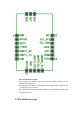
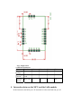
Pin number 1 2 3 Name GND ANT GND Type Power RF Power Description System GND Signal wire System GND 4 5 GND GPIO4/PE7 Power I 6 7 8 9 10 SWIM nTRST UART1_RX UART1_TX PWM/PD0 Debug IO I I O O System GND 1. For the external MCU to wake up LoRa module 2. For the external MCU to let LoRa to know it is ready to receive AT instruction More information see note below. Debug for simulator Reset ,low level signal effective.
21 IIC_SCL/PC1 O IIC SCL 22 AD/PC2 A/IO(PC2) ADC (Analog-digital conversion) Note :I –Input, O-Output, A-Analog (About PE6 and PE7) LoRa module is in dormant mode mostly. If MCU is interact with the module, it needs to wake up LoRa module first and then send AT instruction to LoRa module. Then PE7 (GPI04) is the pin to wake up LoRa module for MCU;Similarly, if the module is interact with the external MCU( Send AT instruction ), it needs to wake up external MCU (then send AT instruction ).
Note:height 2.5mm 3.4 Electrical character Parameter Condition Minimum Working 3 voltage Working Continuous current send dormant RTC work current 4 Normal 3.3 Maximum Unit 3.
instruction to MCU. In order to reduce power consumption, LoRa and MCU are normally in dormant state. Each of them handles its own message. When it needs another, it will wake up another and gives AT instruction to another. When AT instruction are sent on both side, additional course will happen when there are at the same time. Therefore, the design for this is a “half duplex” mode. That is: only one side can send instruction at one time.
In fact, all the AT instruction send form MCU to LoRa will let LoRa to have a corresponding reply (refer to the AT instruction set at the back). So, after MCU sent instruction to LoRa, it can go to dormant, or wait for LoRa to reply before dormant. This reply time, normal in a few ms.( The set of three tuple’s instruction takes long time, around 200 ms). 4.
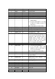
AT+JOIN 5.1.6:Send data AT+DTX=12,313233343536 5.1.7:Receive data (AT+DRX=6,313233) 5.1.8:Time AT+GETRTC AT+SETALARM=20200318140100 5.1.9:Others AT+START AT+VERSION AT+RESTORE 5.2、Note: 1. If in Class A mode, set the three tuple, channel, networking mode in 4.1, Reissue the network instruction ; if in Class B mode, more slot time will be set; 2.
//AT+ APPEUI=1122334455667788 tuple’s AT+ APPKEY=(16 bytes long) information Note:When the equipment leaves the factory, the ternary default value is 0. If the setting is successful, save automatically and the saved value is used to the next start. ( Refer to the APP User Manual for the definition and acquisition of three tuple); APPEUI is not used in three tuple. The reason of ERROR returned after AT : No parameter or wrong parameter length. 5.3.
5.3.4 Set the period of Class B Slot Format Instruction AT+SLOTFREQ=64 Instruction AT+SLOTFREQ=OK / AT+SLOTFREQ=ERROR AT+SLOTFREQ=? Respond AT+SLOTFREQ=64 Respond Note 1,2,4,8,16, 32,64,128,for example 64, means one communication per 64 seconds. The query Return query results Note:The instruction is valid under Class B. Optional value is set as: 1 / 2 / 4 / 8 / 16 / 32 / 64 / 128. The shorter of the setting cycle, the greater power consumption of the module.
OK:begin to access the network SUCC: access the network successfully FAIL: fail to access Respond2 AT+JOIN=FAIL / AT+JOIN=SUCC the network TRANS: into Respond3 AT+JOIN=TRANS ClassB mode Query the current Instruction AT+JOIN=? stage of the network AT+JOIN=[ NONE| JOINING| FAIL| SUCC| The query results Respond WAITBEACON| TRANS] Description Note:The Instruction; should not normally be initiated until the three tuple, Channel, Working Mode and slot cycle’s (Class B required) setting are complete Note: the retu
connected automatically). If successful, enter the normal. If you fail to enter the net, try up to 4 times, then go to 1 hour of sleep, wake up and try 4 more, . .. When automatically, AT JOIN reply output (same as during manual access). The reason of ERROR returned after AT: it is already in the network state or currently in the network. 5.3.
AT+SETALARM=OK /AT+SETALARM=ERROR AT+ALARM=year month day hour minute Respond2 second Note: has 3 reasons for returning to ERROR: 1. The time is not synchronized; Solution: use this AT after the success access of network 2. The setting time is earlier than the present time; Solution: check the time line. 3. The setting time is more than 49days; Solution: make sure the alarm time is within 49 days.
This device complies with Part 15 of the FCC Rules. Operation is subject to the following two conditions: (1) this device may not cause harmful interference, and (2) this device must accept any interference received, including interference that may cause undesired operation. The module is limited to OEM installation ONLY The OEM integrator is responsible for ensuring that the end-user has no manual instruction to remove or install module.