
Datasheet

Rev. 1.0 / Jul. 2012 56
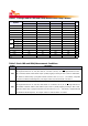
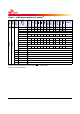
I
DD2N
Precharge Standby Current
CKE: High; External clock: On; tCK, CL: see Table 1; BL: 8
a)
; AL: 0; CS: stable at 1; Command, Address, Bank
Address Inputs: partially toggling according to Table 5; Data IO: MID_LEVEL; DM: stable at 0; Bank Activity: all
banks closed; Output Buffer and RTT: Enabled in Mode Registers
b)
; ODT Signal: stable at 0; Pattern Details:
see Table 5.
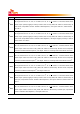
I
DD2NT
Precharge Standby ODT Current
CKE: High; External clock: On; tCK, CL: see Table 1; BL: 8
a)
; AL: 0; CS: stable at 1; Command, Address, Bank
Address Inputs: partially toggling according to Table 6; Data IO: MID_LEVEL; DM: stable at 0; Bank Activity: all
banks closed; Output Buffer and RTT: Enabled in Mode Registers
b)
; ODT Signal: toggling according to Table 6;
Pattern Details: see Table 6.
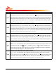
I
DD2P0
Precharge Power-Down Current Slow Exit
CKE: Low; External clock: On; tCK, CL: see Table 1; BL: 8
a)
; AL: 0; CS: stable at 1; Command, Address, Bank
Address Inputs: stable at 0; Data IO: MID_LEVEL; DM: stable at 0; Bank Activity: all banks closed; Output Buf-
fer and RTT: Enabled in Mode Registers
b)
; ODT Signal: stable at 0; Precharge Power Down Mode: Slow Exit
c)
I
DD2P1
Precharge Power-Down Current Fast Exit
CKE: Low; External clock: On; tCK, CL: see Table 1; BL: 8
a)
; AL: 0; CS: stable at 1; Command, Address, Bank
Address Inputs: stable at 0; Data IO: MID_LEVEL; DM: stable at 0; Bank Activity: all banks closed; Output Buf-
fer and RTT: Enabled in Mode Registers
b)
; ODT Signal: stable at 0; Precharge Power Down Mode: Fast Exit
c)
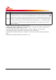
I
DD2Q
Precharge Quiet Standby Current
CKE: High; External clock: On; tCK, CL: see Table 1; BL: 8
a)
; AL: 0; CS: stable at 1; Command, Address, Bank
Address Inputs: stable at 0; Data IO: MID_LEVEL; DM: stable at 0; Bank Activity: all banks closed; Output Buf-
fer and RTT: Enabled in Mode Registers
b)
; ODT Signal: stable at 0
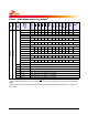
I
DD3N
Active Standby Current
CKE: High; External clock: On; tCK, CL: see Table 1; BL: 8
a)
; AL: 0; CS: stable at 1; Command, Address, Bank
Address Inputs: partially toggling according to Table 5; Data IO: MID_LEVEL; DM: stable at 0; Bank Activity: all
banks open; Output Buffer and RTT: Enabled in Mode Registers
b)
; ODT Signal: stable at 0; Pattern Details: see
Table 5.
I
DD3P
Active Power-Down Current
CKE: Low; External clock: On; tCK, CL: see Table 1; BL: 8
a)
; AL: 0; CS: stable at 1; Command, Address, Bank
Address Inputs: stable at 0; Data IO: MID_LEVEL; DM: stable at 0; Bank Activity: all banks open; Output Buffer
and RTT: Enabled in Mode Registers
b)
; ODT Signal: stable at 0
Symbol Description