
Datasheet


Rev. 1.1 / Aug. 2013 29
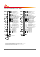
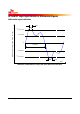
Vref Tolerances
The dc-tolerance limits and ac-noise limits for the reference voltages
VRefCA
and V
RefDQ
are illustrated in
figure below. It shows a valid reference voltage V
Ref
(t) as a function of time. (V
Ref
stands for V
RefCA
and
V
RefDQ
likewise).
V
Ref
(DC) is the linear average of V
Ref
(t) over a very long period of time (e.g. 1 sec). This average has to
meet the min/max requirements in the table "Differential Input Slew Rate Definition" on page 35. Further-
more V
Ref
(t) may temporarily deviate from V
Ref (DC)
by no more than +/- 1% VDD.
Illustration of V
Ref(DC)
tolerance and V
Ref
ac-noise limits
The voltage levels for setup and hold time measurements V
IH(AC)
, V
IH(DC)
, V
IL(AC)
, and V
IL(DC)
are depen-
dent on V
Ref
.
“V
Ref
” shall be understood as V
Ref(DC)
, as defined in figure above.
This clarifies that dc-variations of V
Ref
affect the absolute voltage a signal has to reach to achieve a valid
high or low level and therefore the time to which setup and hold is measured. System timing and voltage
budgets need to account for V
Ref(DC)
deviations from the optimum position within the data-eye of the input
signals.
This also clarifies that the DRAM setup/hold specification and derating values need to include time and
voltage associated with V
Ref
ac-noise. Timing and voltage effects due to ac-noise on V
Ref
up to the speci-
fied limit (+/- 1% of VDD) are included in DRAM timings and their associated deratings.
VDD
VSS
VDD/2
V
Ref(DC)
V
Ref
ac-noise
voltage
time
V
Ref(DC)max
V
Ref(DC)min
V
Ref
(t)