
User's Manual


AMPAK Technology Inc. www.ampak.com.tw Proprietary & Confidential Information
Doc. NO:
8
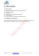
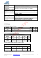
5. Pin Assignments
5.1 PCB Pin Outline
< TOP VIEW >
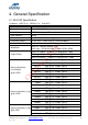
5.2 Pin Definition
NO
Name Type
Description
1 WLAN_ANT I/O
RF signal I/O port
2 GND
-
Ground
3 JTAG_TRST_L I JTAG interface, if JTAG not used unconnected (NC)
4 JTAG_TDO_UART_TX
O
JTAG interface, if JTAG not used unconnected (NC)
this pin. This pin is also muxed with UART_TX,
which can be enabled by software
5 JTAG_TDI_UART_RX
I
JTAG i
nterface, if JTAG not used unconnected (NC)
this pin. This pin is also muxed with UART_RX,
which can be enabled by software
6 JTAG_TCK I JTAG interface, if JTAG not used unconnected (NC)
7 JTAG_TMS I JTAG interface, if JTAG not used unconnected (NC)
8 GND
-
Ground
9 OSC_IN I XTAL oscillator input
10
OSC_OUT I/O
XTAL oscillator output
11
GND
-
Ground
12
RF_SW_CTRL0
-
Floating (Don’t connected to ground)
13
RF_SW_CTRL3
-
Floating (Don’t connected to ground)
Only for TPV.