
User's Manual


AMPAK Technology Inc. www.ampak.com.tw Proprietary & Confidential Information
Doc. NO:
2
Contents
Revision History......................................................................................................... 1
Contents..................................................................................................................... 2
1. Introduction........................................................................................................... 3
2. Features ............................................................................................................... 4
3. Deliverables.......................................................................................................... 5
3.1 Deliverables.................................................................................................... 5
3.2 Regulatory certifications ................................................................................. 5
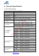
4. General Specification............................................................................................ 6
4.1 Wi-Fi RF Specification .................................................................................... 6
4.2 Voltages.......................................................................................................... 7
4.2.1 Absolute Maximum Ratings.................................................................... 7
4.2.2 Recommended Operating Ratings ......................................................... 7
5. Pin Assignments ................................................................................................... 8
5.1 PCB Pin Outline.............................................................................................. 8
5.2 Pin Definition .................................................................................................. 8
6. Dimensions......................................................................................................... 11
6.1 Physical Dimensions..................................................................................... 11
6.2 Recommended Footprint .............................................................................. 12
7. External clock reference ..................................................................................... 13
7.1 SDIO Pin Description.................................................................................... 13
8. Host Interface Timing Diagram ........................................................................... 14
8.1 Power-up Sequence Timing Diagram ........................................................... 14
8.2 SDIO Default Mode Timing Diagram............................................................. 14
8.3 SDIO High Speed Mode Timing Diagram ..................................................... 15
9. Recommended Reflow Profile ............................................................................ 16
10. Packing Information............................................................................................ 17
10.1 Label........................................................................................................... 17
10.2 Dimension................................................................................................... 18
10.3 MSL Level / Storage Condition ................................................................... 20
Only for TPV.