
User Manual


3.4 Fieldbus Type Address Map
127
(1) PLC Address Composition
(m is PLC input and output top word address for each axis number)
PLC ĺ MSEP (PLC Output) MSEP ĺ PLC (PLC Input)
A2 to A17 m B2 to B17 m
A18 to A33 m+1 B18 to B33 m+1
[Refer to Section 3.4.2 for the address maps for each Fieldbus.]
䎃
(2) Input and Output Signal Assignment for each Axis
The I/O signals for each axis consists of 1-word for each I/O bit register.
Ɣ The I/O bit register is controlled using the ON/OFF signal in units of bit.
(ON = Applicable bit is “1”, OFF = Applicable bit is “0”)
Ɣ Pin Numbers A2 to A33 and B2 to B13 are assigned for each bit signal, which are equivalent
to the case when using PIO, because the contents of signals vary depending on the selection
of PIO pattern.
[Refer to 3.5 Control Signals for PIO Operation for the relation between pin numbers and
signals.]
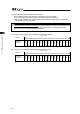
PLC Output (m is PLC input and output top word address for each axis number)
䎃
Address m
b15 b14 b13 b12 b11 b10 b9 b8 b7 b6 b5 b4 b3 b2 b1 b0
Controller Input
Port (Pin) No.
A17
A16
A15
A14
A13
A12
A11
A10
A9
A8
A7
A6
A5
A4
A3
A2
䎃
Address m+1
b15 b14 b13 b12 b11 b10 b9 b8 b7 b6 b5 b4 b3 b2 b1 b0
Controller Input
Port (Pin) No.
A33
A32
A31
A30
A29
A28
A27
A26
A25
A24
A23
A22
A21
A20
A19
A18
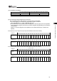
PLC Input (m is PLC input and output top word address for each axis number)
䎃
Address m
F E D C B A 9 8 7 6 5 4 3 2 1 0
Controller Output
Port No.
B17
B16
B15
B14
B13
B12
B11
B10
B9
B8
B7
B6
B5
B4
B3
B2
䎃
Address m+1
F E D C B A 9 8 7 6 5 4 3 2 1 0
Controller Output
Port No.
B33
B32
B31
B30
B29
B28
B27
B26
B25
B24
B23
B22
B21
B20
B19
B18
䎃
1 word = 16 bit