
8-Bit Microcontroller with OTP ROM Specification Sheet


EM78P447N
8-Bit Microcontroller with OTP ROM
10 •
Product Specification (V1.1) 03.30.2005
(This specification is subject to change without further notice)
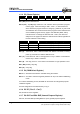
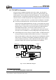
4.1.4 R3 (Status Register)
7 6 5 4 3 2 1 0
GP PS1 PS0 T P Z DC C
Bit 7 (GP) General read/write bit.
Bits 6 (PS1) ~ 5 (PS0) Page select bits. PS1~PS0 are used to pre-select a program
memory page. When executing a "JMP", "CALL", or other instructions
which causes the program counter to change (e.g. MOV R2, A), PS1~PS0
are loaded into the 11th and 12th bits of the program counter and select one
of the available program memory pages. Note that RET (RETL, RETI)
instruction does not change the PS0~PS1 bits. That is, the return will
always be to the page from where the subroutine was called, regardless of
the PS1~PS0 bits current setting.
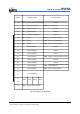
PS1 PS0 Program memory page [Address]
0 0 Page 0 [000-3FF]
0 1 Page 1 [400-7FF]
1 0 Page 2 [800-BFF]
1 1 Page 3 [C00-FFF]
Bit 4 (T) Time-out bit. Set to 1 with the "SLEP" and "WDTC" commands, or during
power up, and reset to 0 with the WDT time-out.
Bit 3 (P) Power down bit. Set to 1 during power on or by a "WDTC" command and
reset to 0 by a "SLEP" command.
Bit 2 (Z) Zero flag. Set to "1" if the result of an arithmetic or logic operation is zero.
Bit 1 (DC) Auxiliary carry flag.
Bit 0 (C) Carry flag
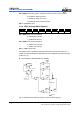
4.1.5 R4 (RAM Select Register)
Bits 7~6 determine which bank is activated among the 4 banks.
Bits 5~0 are used to select the registers (address: 00~3F) in the indirect addressing
mode.
If no indirect addressing is used, the RSR can be used as an 8-bit general-purpose
read/writer register.
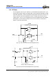
See the configuration of the data memory in Fig. 4.
4.1.6 R5~R7 (Port 5 ~ Port7)
R5, R6 and R7 are I/O registers
4.1.7 R8~R1F and R20~R3E (General Purpose Register)
R8~R1F, and R20~R3E (including Banks 0~3) are general-purpose registers.