CMX58886CX cpuModules™ User’s Manual BDM-610000050 Revision A PRELIMINARY ® www.rtd.
CMX58886CX cpuModules™ User’s Manual RTD Document Number: BDM-610000050 Revision A Copyright © 2006 RTD Embedded Technologies, Inc. All rights reserved. Trademarks Advanced Digital I/O, aDIO, a2DIO, Autonomous SmartCal, cpuModule, dspFramework, dspModule, IDAN, HiDAN, HiDANplus, “MIL Value for COTS prices”, multiPort, and PC/104EZ are trademarks, and “Accessing the Analog World”, dataModule, RTD, and the RTD logo are registered trademarks of RTD Embedded Technologies, Inc.
CMX58886CX cpuModules™ ® www.rtd.
iv CMX58886CX cpuModule BDM-610000050 Rev A
Table of Contents Chapter 1 Introduction CMX58886CX cpuModules . . . . . . . . . . . . . . . . . . . . . . . . . . . . . . . . . . . . . . . . . . . . . . . . . . . . . . . . . . . . . . . . . . . . . . . . . . . . 2 Thermal Monitor and Thermal Throttling . . . . . . . . . . . . . . . . . . . . . . . . . . . . . . . . . . . . . . . . . . . . . . . . . . . . . . . . . . . . . . . . . . . . Error-Correction Codes . . . . . . . . . . . . . . . . . . . . . . . . . . . . . . . . . . . . . . . . . . . . . . .
Battery . . . . . . . . . . . . . . . . . . . . . . . . . . . . . . . . . . . . . . . . . . . . . . . . . . . . . . . . . . . . . . . . . . . . . . . . . . . . . . . . . . . . . . . . . . . . . . . . . . . . . . 28 SVGA Video Connector (CN18) . . . . . . . . . . . . . . . . . . . . . . . . . . . . . . . . . . . . . . . . . . . . . . . . . . . . . . . . . . . . . . . . . . . . . . . 29 LVDS Flat Panel Video Connector (CN19) . . . . . . . . . . . . . . . . . . . . . . . . . . . . . . . . . . . . . . . . .
multiPort: Advanced Digital I/O Ports (aDIO™) . . . . . . . . . . . . . . . . . . . . . . . . . . . . . . . . . . . . . . . . . . . . . . . . . . . . . . . 56 Digital I/O Register Set . . . . . . . . . . . . . . . . . . . . . . . . . . . . . . . . . . . . . . . . . . . . . . . . . . . . . . . . . . . . . . . . . . . . . . . . . . . . . . . . . . . . . . . Port 1 Data register is a read/write byte direction . . . . . . . . . . . . . . . . . . . . . . . . . . . . . . . . . . . . . . . . . . . . . . . . . .
NVRAM Updates . . . . . . . . . . . . . . . . . . . . . . . . . . . . . . . . . . . . . . . . . . . . . . . . . . . . . . . . . . . . . . . . . . . . . . . . . . . . . . . . . . . . . . . . . . . . Boot Device Order . . . . . . . . . . . . . . . . . . . . . . . . . . . . . . . . . . . . . . . . . . . . . . . . . . . . . . . . . . . . . . . . . . . . . . . . . . . . . . . . . . . . . . . . . . . 74 74 System Recovery. . . . . . . . . . . . . . . . . . . . . . . . . . . . . . . . . . . . . . . . . . . . . .
Chapter 1 Introduction This manual provides comprehensive hardware and software information for users developing with the CMX58886CX PC/104-Plus cpuModule. Note Read the specifications beginning on page 10 prior to designing with the cpuModule.
CMX58886CX cpuModules RTD's CMX58886CX cpuModule represents the latest in high-performance embedded computing solutions. It includes 400 MHz source-synchronous Front Side Bus (FSB), on-die 512kB L2 cache, and data pre-fetch logic. It uses a 333MHz DDR-SDRAM controller that can support up to 2.7 G-Bytes per second of memory bandwidth. All memory chips are soldered directly onto the board. The video interface is provided by an Analog SVGA output and an LVDS flat panel output.
Thermal Monitor and Thermal Throttling The Intel ® Thermal Monitor is a feature on the CMX58886CX that automatically throttles the CPU when the CPU exceeds its thermal limit. The maximum temperature of the processor is defined as the temperature that the Thermal Monitor is activated. The thermal limit and duty cycle of the Thermal Monitor cannot be modified. The Thermal Monitor can be disabled by the BIOS for applications where deteministic speed is more important than device failure due to thermal runaway.
aDIO with Wake-on-aDIO RTD’s exclusive multiPort™ allows the parallel port to be configured as an Advanced Digital I/O (aDIO™), ECP/ EPP parallel port, or a floppy drive. aDIO™ is 16 digital bits configured as 8 bit-direction programmable and 8-bit port-direction programmable I/O giving you any combination of inputs and outputs. Match, event, and strobe interrupt modes mean no more wasting valuable processor time polling digital inputs.
Ordering Information The CMX58886CX cpuModule is available with a 1.0 GHz processor and 256 or 512 MB of DDR SDRAM. The cpuModule can also be purchased as part of an Intelligent Data Acquisition Node (IDAN™) building block, which consists of the cpuModule and a milled aluminum IDAN frame. The IDAN building block can be used in just about any combination with other IDAN building blocks to create a simple but rugged PC/104 stack. Refer to Appendix C, IDAN™ Dimensions and Pinout, for more information.
Board Features • 1.0 GHz Intel Celeron M with thermal throttling – 400 MHz, source-synchronous Front Side Bus – Math coprocessor • – Internal Cache • • • • • • 6 L1 - 32KB of instruction and 32KB data; L2 - 512kB 256 or 512 Mbytes BGA DDR SDRAM – Up to 333 MHz Data Rate – ECC corrects single-bit memory errors and detects 2-bit errors Stackable 120-pin PCI bus – 4 Bus master add-on cards capable – 3.
I/O • • AC97 Audio Support – Selectable Headphone or Line level output – Line level input – Microphone input Fast Ethernet – Ethernet Controller • • – • • Full Duplex support Low Power Features LED Status Software configuration 855GME SVGA controller Onboard with 3D Acceleration – DirectX & OpenGL 3D Accelerator – Analog SVGA Output – LVDS Flat Panel output – Resolution up to 2048 x 1536 pixels with 32K colors – VGA, SVGA, XGA, SXGA, UXGA – Up to 16 million colors – 64-bit AGP Har
• • • • • Two USB 2.0 (Universal Serial Bus) Ports – Supports 480 Mb/s (high-speed), 12Mb/s (full-speed), and 1.
Block Diagram The next figure shows a simplified block diagram of the CMX58886CX cpuModule. Intel Pentium M 1.4/1.1 GHz 855 GME NorthBridge DDR SDRAM 333 MHz w/ ECC SVGA/ LVDS Flat Panel 2 x USB 2.
Specifications Physical Characteristics • • • Dimensions: 117mm L x 97mm W x 15mm H (4.6"L x 3.8"W x 0.6"H) Weight: Approximately 0.19 Kg (0.40 lbs.) PCB: 14-layer, mixed surface-mount and thru-hole Power Consumption Exact power consumption depends on the actual application. Table 2 lists power consumption for typical configurations and clock speeds. Table 2 cpuModule Power Consumption Module Speed RAM Power, typ. Power, Max. CMX58886CX 1.0 GHz 256 or 512 MB 10.9 W 12.
Electrical Characteristics The table below lists the Electrical Characteristics of the CMX58886CX. Operating outside of these parameters may cause permanent damage to the cpuModule. Table 4 Symbol Electrical Characteristics Parameter Test Condition Min. Max. PCI VOH Output Voltage High IOH = –0.5 mA 2.9 V 3.3 V VOL Output Voltage Low IOL = 6.0 mA 0.0 V 0.55 V VIH Input Voltage High — 1.8 V 5.5 V VIL Input Voltage Low — -0.5 V 0.
Table 4 Symbol Electrical Characteristics Parameter Test Condition Min. Max. SVGA Port VOH Output Voltage High HSYNC, VSYNC IOH = –32.0 mA 3.8 V 5.0 V VOL Output Voltage Low HSYNC, VSYNC IOL = 32.0 mA 0.0 V 0.55 V VOH Output Voltage High DDC_* IOH = –4.0 mA 2.4 V 3.3 V VOL Output Voltage Low DDC_* IOL = 8.0 mA 0.0 V 0.4 V VIH Input Voltage High DDC_* — 2.0 V 5.5 V VIL Input Voltage Low DDC_* — -0.3 V 0.
Contact Information RTD Embedded Technologies, Inc. 103 Innovation Blvd. State College, PA 16803-0906 USA Phone: Fax: +1-814-234-8087 +1-814-234-5218 E-mail: sales@rtd.com techsupport@rtd.com Internet: http://www.rtd.
14 CMX58886CX cpuModule BDM-610000050 Rev A
Chapter 2 Getting Started For many users, the factory configuration of the CMX58886CX cpuModule can be used to get a PC/104 system operational. You can get your system up and running quickly by following the simple steps described in this chapter, which are: 1. Connect power. 2. Connect the utility harness. 3. Connect a keyboard. 4. Default BIOS configuration. 5. Fail Safe Boot ROM. 6. Connect a VGA monitor to the SVGA connector.
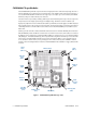
Connector Locations Figure 3 shows the connectors and the ATA/IDE Disk Chip socket of the CMX58886CX cpuModule. SVGA Video (CN18) CN14 CN12 PCI Bus (CN16) Audio (CN11) LVDS Flat Panel (CN19) COM1 (CN7) CN15 COM2 (CN8) USB 2.
Table 5 CMX58886CX Basic Connectors Connector Function Size CN3 Auxiliary Power 12-pin CN4 Bridge Link 4-pin CN5 Utility Port 10-pin CN6 multiPort 26-pin CN7 Serial Port 1 (COM1) 10-pin CN8 Serial Port 2 (COM2) 10-pin CN9 Reserved 10-pin CN10 EIDE Connector 44-pin CN11 Audio Connector 10-pin CN12 External Power Management 3-pin CN13 RTC Battery Input (optional) 2-pin CN14 Fan Power (+5V) 2-pin CN15 Fan Power (switched) 2-pin CN16 PC/104-Plus (PCI) Bus 120-pin CN1
Connecting the Utility Cable The multi-function connector (CN5) implements the following interfaces: • • • • • • PC/AT compatible keyboard PS/2 mouse port Speaker port (0.1W output) Hardware Reset input Battery input for Real Time Clock Soft Power Button input To use these interfaces, you must connect to the utility port connector (CN5).
• • PCI bus expansion card power PCI bus signaling levels Slot Selection Switches Unlike PC/104 cards, PC/104-Plus and PCI-104 expansion cards have a "slot" selection switch or jumpers. In total, there are 4 PCI cards that can be stacked onto the cpuModule with switch positions 0 through 3. The distance from the CPU determines these switch settings. The card closest to the CPU is said to be in slot 0, the next closest slot 1 and so on to the final card as slot 3.
Booting the CMX58886CX cpuModule for the First Time You can now apply power to the cpuModule. You will see: • • • A greeting message from the VGA BIOS (if the VGA BIOS has a sign-on message) The cpuModule BIOS version information A message requesting you press Delete to enter the Setup program If you don’t press Delete, the cpuModule will try to boot from the current settings. If you press Delete, the cpuModule will enter Setup.
Chapter 3 Connecting the cpuModule This chapter provides information on all CMX58886CX cpuModule connectors. Connector Locations —page 22 Auxiliary Power (CN3)—page 24 Utility Port Connector (CN5)—page 26 SVGA Video Connector (CN18)—page 29 LVDS Flat Panel Video Connector (CN19)—page 31 EIDE Connector (CN10)—page 32 ATA/IDE Disk Chip Socket (U16)—page 33 Serial Port 1 (CN7) and Serial Port 2 (CN8)—page 34 multiPort™ (CN6)—page 37 USB 2.
Connector Locations Figure 4 shows the connectors and the ATA/IDE Disk Chip socket of the CMX58886CX cpuModule. SVGA Video (CN18) CN14 CN12 PCI Bus (CN16) Audio (CN11) LVDS Flat Panel (CN19) COM1 (CN7) CN15 COM2 (CN8) USB 2.
Table 6 CMX58886CX Basic Connectors BDM-610000050 Rev A Connector Function Size CN3 Auxiliary Power 12-pin CN4 Bridge Link 4-pin CN5 Utility Port 10-pin CN6 multiPort 26-pin CN7 Serial Port 1 (COM1) 10-pin CN8 Serial Port 2 (COM2) 10-pin CN9 Reserved 10-pin CN10 EIDE Connector 44-pin CN11 Audio Connector 10-pin CN12 External Power Management 3-pin CN13 RTC Battery Input (optional) 2-pin CN14 Fan Power (+5 V) 2-pin CN15 Fan Power (switched) 2-pin CN16 PC/104-Plus
Auxiliary Power (CN3) WARNING If you connect power incorrectly, the module will almost certainly be destroyed. Please verify power connections to the module before applying power. Power can be conveyed to the module either through the PCI-104-Plus bus (CN16) or through the Auxiliary Power connector (CN3). The cpuModule only requires +5 VDC and ground for operation; however, other modules in the system may require +12 VDC, –12 VDC, and –5 VDC.
Facing the connector pins, the pinout of the Auxiliary Power connector is: 11 9 7 5 3 1 PSON# GND GND Reserved +5V_STDBY GND +3.3 V +3.3 V +5 V –12 V +12 V +5 V 12 10 8 6 4 2 Power Supply Protection The cpuModule has protection circuitry that helps prevent damage due to problems with the +5 V supply, such as reversed polarity, overvoltage, and overcurrent.
Utility Port Connector (CN5) The utility port connector implements the following functions: • • • • • • PC/AT compatible keyboard port PS/2 mouse port Speaker port (0.1W output) Hardware Reset input Battery input for Real Time Clock Soft Power Button input Table 8 provides the pinout of the multi-function connector.
Keyboard A PS/2 compatible keyboard can be connected to the multi-function connector. Usually PC keyboards come with a cable ending with a 5-pin male PS/2 connector. Table 9 lists the relationship between the multi-function connector pins and a standard PS/2 keyboard connector.
Battery Pin 9 of the multi-function connector is the connection for an external backup battery. This battery is used by the cpuModule when system power is removed in order to preserve the date and time in the real time clock. Connecting a battery is only required to maintain time when power is completely removed from the cpuModule. A battery is not required for board operation.
SVGA Video Connector (CN18) Table 11 provides the pinout of the video connector.
The following table lists the supported video resolutions.
LVDS Flat Panel Video Connector (CN19) Table 13 provides the pinout of the Flat Panel Video connector (CN19). FP_VCC can be either +5 V or +3.3 V, and is selected with jumper JP8. FP_VBKLT can be either +5 V or +12 V, and can be selected with JP9. See Jumper Settings and Locations on page 80 for more details.
EIDE Connector (CN10) The EIDE connector is a 44-pin, 2 mm connector that can connect to a variety of EIDE or IDE devices. The connector provides all signals and power needed to use a 2.5-inch form factor (laptop) hard drive. Also, the first 40 pins of the connector provide all of the signals needed to interface to a 3.5-inch or 5-inch form factor hard drive, CD-ROM drive, or other EIDE device. The larger form factors use a 40-pin, 0.
ATA/IDE Disk Chip Socket (U16) The ATA/IDE Disk Chip socket is a 32-pin socket that supports +3.3V or +5V miniature ATA/IDE flash disk chips. The socket allows a true IDE device to be attached to the board with either a socketed or soldered connection. Such true IDE devices are supported by all major operating systems, and do not require special drivers. The socket supports ATA/IDE flash disk chips with capacites up to 4GB..
Serial Port 1 (CN7) and Serial Port 2 (CN8) Serial Port 1 (COM1) is implemented on connector CN7, and Serial Port 2 is implemented on connector CN8. The serial ports are normally configured as PC compatible full-duplex RS-232 ports, but you may use the Setup program to reconfigure these ports as half-duplex RS-422 or full-duplex RS-422 or RS-485. If you reconfigure the ports, you must also select the I/O address and corresponding interrupt using Setup.
Facing the serial port’s connector pins, the pinout is: 9 7 5 3 1 GND DTR TXD RXD DCD GND RI CTS RTS DSR 10 8 6 4 2 RS-422 or RS-485 Serial Port You may use Setup to configure the serial ports as RS-422 or RS-485. In this case, you must connect the serial port to an RS-422 or RS-485 compatible device. When using RS-422 or RS-485 mode, you can use the serial ports in either half-duplex (two-wire) or full-duplex (four-wire) configurations.
RS-422 and RS-485 Mode Pinout Table 21 provides the serial port connector pinout when RS-422 or RS-485 modes are enabled.
multiPort™ (CN6) RTD’s exclusive multiPort can be configured as an Advanced Digital I/O (aDIO™), a parallel port, or a floppy drive. Refer to Chapter 4, Using the cpuModule, to configure the multiPort. multiPort Configured as an Advanced Digital I/O (aDIO™) Port The mulitPort connector (CN6) can be configured as an aDIO port. aDIO is 16 digital bits configured as 8-bit programmable and 8-bit port programmable I/O, providing any combination of inputs and outputs.
multiPort Configured as a Parallel Port The parallel port is available on connector CN6. Make sure the multiPort in the BIOS Setup is configured to parallel port. You can use the BIOS Setup to select the parallel port’s address and associated interrupt, and choose between its operational modes (SPP, ECP, EPP 1.7, and EPP 1.9). The pinout of the connector enables a ribbon cable to be connected directly to a DB-25 connector, thus providing a standard PC compatible port.
multiPort Configured as a Floppy Drive Controller The multiPort (CN6) can be configured to be a floppy drive controller. This can be configured in the BIOS Setup under Integrated Peripherals. For more information on configuring the multiPort in the BIOS Setep, refer to page 60 Table 24 shows the pin assignments to connect a floppy drive to the multiPort.
USB 2.0 Connector (CN17) Two USB 2.0 compliant connectors are available on connector, CN17. Table 25 provides the pinout of the USB connector.
Ethernet (10/100Base-T and -TX) Connector (CN20) The functionality of the Ethernet port is based on the Intel 82562 Fast Ethernet PCI controller. Table 27 provides the pinout of the Ethernet connector.
Audio (CN11) A full featured AC97 compliant audio port is available on CN11. It provides a mono microphone input, stereo line level input, and a stereo output that can be configured as line level or headphone level. The output is configured in the BIOS setup utility. When used as a headphone output, it will drive 32 Ohm speaker at 50mW. Table 27 Audio Connector (CN11) 10-Pin DIL Pin 42 Signal Function In/Out 1 MIC_VREF 2.2V Supply to bias microphones. 5mA max. 2 MIC_IN Microphone input.
PC/104-Plus PCI Bus (CN16) Connector CN16 carries the signals of the PC/104-Plus PCI bus. These signals match definitions of the PCI Local Bus specification Revision 2.1. Table 28 list the pinouts of the PC/104-Plus bus connector. Table 28 PC/104-Plus Bus Signal Assignments1 Pin A B C D 1 GND Reserved/+5V_STDBY2 +5 V AD00 2 VIO AD02 AD01 +5 V 3 AD05 GND AD04 AD03 4 C/BE0# AD07 GND AD06 5 GND AD09 AD08 GND 6 AD11 VIO AD10 M66EN 7 AD14 AD13 GND AD12 8 +3.
PC/104-Plus PCI Bus Signals The following are brief descriptions of the PC/104-Plus PCI bus signals. Address and Data AD[31:00] — Address and Data are multiplexed. A bus transaction consists of an address cycle followed by one or more data cycles. C/BE[3:0]# — Bus Command/Byte Enables are multiplexed. During the address cycle, the command is defined. During the Data cycle, they define the byte enables. PAR — Parity is even on AD[31:00] and C/BE[3:0]# and is required.
Power Supplies and VIO +5 V — +5 V supply connected to PC/104 bus and auxiliary power connector (CN3) +5 V supplies. +12 V — +12 V supply connected to PC/104 bus and auxiliary power connector (CN3) +12 V supplies. –12 V — –12 V supply connected to PC/104 bus and auxiliary power connector (CN3) –12 V supplies. +3.3 V — The +3.3 V pins on the PC/104-Plus (PCI) connector may be supplied by the onboard +3.3V power supply, however this is not the the default configuration. To supply +3.
Bridge Link (CN4) The Bridge Link connector allows devices that requires Legacy/ISA interrupts to inteface with the cpuModule. When ISA devices are installed in the system (via a PCI to ISA bridge card), the Bridge Link connector provides Legacy/ISA DMA request signals, as well as a serial interrupt signal which permits access to all available system interrupts. Multiple devices may utilize the serial interrupt signal, SERIRQ, which is decoded on the cpuModule.
External Power Management (CN12) An external power management connector (CN12) is available for external devices to wake the system from low power states. Some low power modes require that +5 V standby power is applied to the cpuModule during the wake event. For more information on power management, including a description of the board’s supported wake options, refer to the Power Management section on page 66.
Fan Power, Switched (CN15) The switched fan power connector (CN15) is an optional fan connector which allows the system to power the fan only when the processor temperature reaches high temperatures. To utilize this connector, refer to the Thermal Management section on page 65.
Chapter 4 Using the cpuModule This chapter provides information for users who wish to develop their own applications programs for the CMX58886CX cpuModule.
The RTD Enhanced AMI BIOS The RTD Enhanced AMI BIOS is software that interfaces hardware-specific features of the cpuModule to an operating system (OS). Physically, the BIOS software is stored in a Flash EPROM on the cpuModule. Functions of the BIOS are divided into two parts. The first part of the BIOS is known as POST (power-on self-test) software, and it is active from the time power is applied until an OS boots (begins execution).
Main Menu Setup Fields The following is a list of Main Menu Setup fields.
Booting to Boot Block Flash with Fail Safe Boot ROM Note Boards are shipped with Fail Safe Boot ROM enabled. When Fail Safe Boot ROM is enabled, the system will boot to it exclusively. The Fail Safe Boot ROM is a minimal build of ROM-DOS™ located inside a surface-mounted Boot Block Flash chip. Boot Block Flash is a write-protected flash device that contains the BIOS and extra room where the Fail Safe Boot ROM is stored.
Memory Map The ISA portion of the cpuModule addresses memory using 24 address lines. This allows a maximum of 224 locations, or 16 MB of memory. Table 36 shows how memory in the first megabyte is allocated in the system. Table 36 First Megabyte Memory Map Address (hex) Description C0000–FFFFFh ROM 256 KB BIOS in Flash EPROM, shadowed into DRAM during runtime. C0000–EFFFFh Run time user memory space. Usually, memory between C0000h and CFFFFh is used for the BIOS of add-on VGA video cards.
I/O Address Map As with all standard PC/104 boards, the I/O space is addressed by 10 address lines (SA0–SA9). This allows 210 or 1024 distinct I/O addresses. Any add-on modules you install must therefore use I/O addresses in the range of 0–1023 (decimal) or 000–3FF (hex). Note If you add any PC/104 modules or other peripherals to the system you must ensure they do not use reserved addresses listed below, or malfunctions will occur. The exception to this is if the resource has been released by the user.
Hardware Interrupts Note If you add any expansion modules or other peripherals to the system, you must ensure they do not use interrupts needed by the cpuModule, or malfunctions will occur. The CMX58886CX cpuModule supports the standard PC interrupts listed in Table 38. Interrupts not in use by hardware on the cpuModule itself are listed as available. Similarly, if the operating system is using APIC, more IRQs will be available.
multiPort: Advanced Digital I/O Ports (aDIO™) Ensure that the BIOS setup has the multiPort set to aDIO mode. This board supports 16 bits of TTL/CMOS compatible digital I/O (TTL signaling). Use the BIOS setup to set the multiPort into its aDIO mode. These I/O lines are grouped into two ports, Port 0 and Port 1. Port 0 is bit programmable; Port 1 is byte programmable. Port 0 supports RTD’s Advanced Digital Interrupt modes. The two modes are match and event.
Table 42 DIO-Control I/O Address 453h—Read Access D7 D6 D5 D4 Strobe 1 Status 0 = no strobe 1 = strobe Strobe 0 Status 0 = no strobe 1 = strobe Digital IRQ Status 0 = no digital interrupt 1 = digital interrupt D3 Digital IRQ Mode 00 = Disabled 01 = strobe Mode 10 = event mode 11 = match mode D2 D1 D0 Multi-Function Register Select 00 = clear mode 01 = port 0 direction 10 = mask register 11 = compare register Port 1 Direction 0 = input 1 = output Table 43 DIO-Control I/O Address 453h—Write Acce
Table 45 Wake Control I/O Address 451h D7 D6 D5 D4 D3 D2 Reserved D1 D0 Int Mask 1 = Interrupt is masked 0=Interrupt is enabled Wake Enable 1=Interrupt triggers a Wake Event 0=Interrupt does not trigger a wake event. Port 1 Data register is a read/write byte direction Interrupts In order to use an interrupt with aDIO, the interrupt must first be selected in the BIOS setup utility under Advanced, I/O Devices, aDIO Configuration, aDIO Interrupt.
Figure 5 aDIO Match Mode Strobe Mode Another interrupt mode supported by aDIO is Strobe mode. This allows the strobe pin of the DIO connector to trigger an interrupt. A low to high transition on the strobe pin will cause an interrupt request. The request will remain high until the Clear Register is read from. Additionally, the Compare Register latched in the value at Port 0 when the Strobe pin made a low to high transition. No further strobes will be available until a read of the Compare Register is made.
multiPort: Parallel Port Control The parallel port may be operated in SPP (output-only), EPP (bidirectional), and ECP (extended capabilities) modes. The mode may be selected in the BIOS, or by application software. To configure the parallel port in the BIOS, enter the BIOS, and follow the steps below: 1. Under the “Advanced” menu in the BIOS, select the “I/O Device Configuration” submenu 2. Set the multiPort mode to “Parallel Port” 3.
IDE Controller Configuration The CPU’s onboard EIDE connector (CN10) supports several different drive speed modes, which are BIOS configurable. Supported drive modes will depend on whether a 40-conductor or 80-conductor cable is connecting the EIDE device. The modes and cable detection schemes described below may be set in the BIOS Setup. Similarly, the ATA/IDE Disk Chip socket (U16) is BIOS configurable.
Legacy Mode and Native Mode IDE The onboard EIDE controller may be configured as a either a Legacy or Native Mode IDE controller in the BIOS Setup. However, the operating system must support the selected mode for the device to operate correctly. The default configuration for the controller is Legacy Mode, as this is supported by most operating systems. Legacy Mode Legacy mode is the default configuration of the onboard EIDE controller.
Real Time Clock Control The cpuModule is equipped with a real time clock (RTC) which provides system date and time functions, and also provides 128 nonvolatile memory locations. The contents of these memory locations are retained whenever an external backup battery is connected, whether or not system power is connected. You may access the RTC date, time, and memory using an index and data register at I/O addresses 70h and 71h. Address 70h is the Index register.
Watchdog Timer Control The cpuModule includes a watchdog timer, which provides protection against programs "hanging", or getting stuck in an execution loop where they cannot respond correctly. When enabled, the watchdog timer must be periodically reset by your application program. If it is not refreshed before the time-out period expires, it will cause a hardware reset of the cpuModule. The watchdog time-out period is typically 1.1 seconds, but can vary between 550 ms and 1.65 seconds.
Thermal Management The cpuModule has several thermal features which can be used to monitor and control the board’s temperature when extreme operating conditions are prevalent. Thermal Monitor and Thermal Throttling The Intel ® Thermal Monitor is a feature on the CMX58886CX that automatically throttles the CPU when the CPU exceeds its thermal limit. The maximum temperature of the processor is defined as the temperature that the Thermal Monitor is activated.
Power Management The CMX58886CX cpuModule supports various powering mechanisms which allow the cpuModule to monitor power consumption and temperature, and achieve minial power consumption states. These unique features include thermal monitoring and thermal throttling, as well as low power modes including APM and ACPI configurations. Various wake options are also available to resume normal system power when power modes are no longer necessary for the application.
• Resume on RTC Alarm: The RTC Alarm allows the system to turn on at a certain time every day. This option is BIOS configurable. AT vs. ATX Power Supplies Both AT and ATX power supplies may be used with the CMX58886CX cpuModule, however AT power supplies do not provide any standby power to the cpuModule. When an AT power supply is used to power the system, low power modes that require a standby power to wake the system will not be fully supported.
Reducing Power Consumption In addition to the CPU’s low power modes, power consumption can further be reduced by making some modifications to the BIOS setup. When the following features are modified, the CPU’s power consumption will descrease: 68 • Memory Speed: Changing the DDR DRAM clock frequency will reduce power consumption, however memory performance will also be reduced.
Multi-Color LED The CMX58886CX has a Multi-Color LED located beside the EIDE connector (CN10) which can be enabled or disabled in the BIOS setup screen. The color of the LED indicates the status of the board, as shown in Table 49.
. 70 CMX58886CX cpuModule BDM-610000050 Rev A
Reset Status Register The cpuModule has several different signals on board which can cause a system reset. If a reset occurs, the reset status register can be used to see which reset or resets have been asserted on the cpuModule. The user has the ability to see which resets have been asserted. Resets can also be cleared. • Examine Resets: Reading from I/O port 0x457 will indicate if a reset has been asserted. If a 1 is read, the corresponding reset has been assserted.
Table 54 Reset Status Description and Priorites I/O Address 457h Reset Signal Reset Priority1 Description D7 Main Power (+5V) 2 Main input power to cpuModule (+5V) D6 CPU Core Power 3 CPU core powers supply D5 Non-Standby Power 3 Power supplies that are not for standby power D4 Memory Power 3 Power to onboard memory banks D3 Standby Power 1 Standby power supplies D2 Reserved - Reserved D1 PCI Reset 4 PCI bus reset signal D0 Utility Reset - Utiliy connector push button rese
User EEPROM A 512kB serial EEPROM (Atmel AT93C66) is available on the cpuModule for the user to save nonvolatile parameters on the cpuModule. The EEPROM can be accessed by reading and writting to I/O address 456h, as shown in the following table.
Features and Settings That Can Affect Boot Time The boot time of a system is dependent upon numerous system settings as well as devices attached to a system.. This section addresses some devices and settings that can increase or decrease a system’s boot time. Quick Boot The BIOS contains a Quick Boot option that minimizes the boot time of the system.
System Recovery Loading Default BIOS Settings The default BIOS can be restored either by using the “Load Defaults” option in the BIOS, or by installing jumper JP5 (see Figure 6 on page 81). In most cases, the easiest way to load default settings is by setting them in the BIOS. For other unique cases, jumper JP5 provides an alternative method of restoring the BIOS settings. To restore the default BIOS settings with jumper JP5, follow the procedure below. 1. Remove power from the system. 2. Install JP5.
Basic Interrupt Information for Programmers An interrupt is a subroutine called asynchronously by external hardware (usually an I/O device) during the execution of another application. The CPU halts execution of its current process by saving the system state and next instruction, and then jumps to the interrupt service routine, executes it, loads the saved system state and saved next instruction, and continues execution. Interrupts are good for handling infrequent events such as keyboard activity.
Intel 8259 Programmable Interrupt Controller The chip responsible for handling interrupt requests in the PC is the Intel 8259 Programmable Interrupt Controller. To use interrupts, you need to know how to read and set the Intel 8259’s interrupt mask register (IMR) and how to send the end-of-interrupt (EOI) command to the Intel 8259. Each bit in the IMR contains the mask status of an IRQ line; bit 0 is for IRQ0, bit 1 is for IRQ1, and so on.
78 CMX58886CX cpuModule BDM-610000050 Rev A
Appendix A Hardware Reference This appendix provides information on CMX58886CX cpuModule hardware, including: Jumper Settings and Locations—page 80 Onboard PCI Devices—page 83 Physical Dimensions—page 84 BDM-610000050 Rev A Appendix A: Hardware Reference 79
Jumper Settings and Locations Many cpuModule options are configured by positioning jumpers. Jumpers are labeled on the board as JP followed by a number.
B1 JP1 B3 JP6 JP5 JP9 JP8 JP2 B2 B7 JP4 Figure 6 CMX58886CX Jumper and Solder Blob Locations (top side) Table 57 Jumper Pins CMX58886CX Jumpers Function Default JP1 2 Enable/disable 120 Ω series termination to COM1 (CN7) in RS-422/485 modes open JP2 2 Enable/disable 120 Ω series termination to COM2 (CN8) in RS-422/485 modes open JP4 3 Select power for the ATA/IDE Disk Chip pins 1–2: +5 V pins 2–3: +3.
Table 58 Solder Blob 82 Positions CMX58886CX Solder Blobs Function Default B1 3 Connect the PCI VI/O to either +3.3 V or +5 V positions 1–2: +5 V positions 2–3: +3.3 V pins 2–3 B2 2 Solder closed to connect USB ground to frame ground open B3 3 Solder jumper B3 can connect +3.3 V on the PCI bus to either the onboard +3.3V or to the board’s +3.3 V supply pins on the auxiliary power connector (CN3). positions 1–2: connect PCI +3.3 V to CN3, pins 10 and 12 positions 2–3: connect PCI +3.
Onboard PCI Devices The CMX58886CX cpuModule has several onboard PCI devices, all of which are listed in the table below.
Physical Dimensions Figure 7 shows the mechanical dimensions of the CMX58886CX cpuModule. Figure 7 CMX58886CX Physical Dimensions (±0.
Appendix B Troubleshooting Many problems you may encounter with operation of your CMX58886CX cpuModule are due to common errors. This appendix includes the following sections to help you get your system operating properly.
Common Problems and Solutions Table 60 lists some of the common problems you may encounter while using your CMX58886CX cpuModule, and suggests possible solutions. If you are having problems with your cpuModule, review this table before contacting RTD Technical Support.
Table 60 Troubleshooting (cont’d) Problem Cause Solution keyboard does not work keyboard interface damaged by misconnection • check if keyboard LEDs light wrong keyboard type • verify keyboard is an “AT” type or switch to “AT” mode floppy drive light always on cable misconnected • check for floppy drive cable connected backwards two hard drives will not work, but one does both drives configured for master • set one drive for master and the other for slave operation (consult floppy does not w
How to Obtain Technical Support If after following the above steps, you still cannot resolve a problem with your CMX58886CX cpuModule, please gather the following information: • • • • • • cpuModule model, BIOS version, and serial number List of all boards in system List of settings from cpuModule Setup program Printout of autoexec.bat and config.
Appendix C IDAN™ Dimensions and Pinout cpuModules, like all other RTD PC/PCI-104 modules, can be packaged in Intelligent Data Acquisition Node (IDAN) frames, which are milled aluminum frames with integrated heat sinks and heat pipes for fanless operation. RTD modules installed in IDAN frames are called building blocks. IDAN building blocks maintain the simple but rugged PC/104 stacking concept.
IDAN Dimensions and Connectors 6-pin mini-DIN (female) module P/N: Adam Tech MDE006W mating P/N: Adam Tech MDP006 9-pin D (male) module P/N: Adam Tech DE09PD mating P/N: Adam Tech DE09SD FRONT 25-pin D (female) module P/N: Adam Tech DB25SD mating P/N: Adam Tech DB25PD 20-pin mini D (female) module P/N: 3M 10220-6212VC mating P/N: 3M 10120-3000VE 9-pin D (female) module P/N: Adam Tech DE09SD mating P/N: Adam Tech DE09PD 15-pin high-density D (female) module P/N: Adam Tech HDT15SD mating P/N: Adam Tech HD
External I/O Connections Table 61 PS/2 Mouse — 6-Pin mini-DIN Connector (female) IDAN Pin # Signal Function 1 MDAT Mouse Data 2 Reserved — 3 GND Ground 4 +5 V +5 Volts 5 MCLK Mouse Clock 6 Reserved — Table 62 Keyboard — 6-Pin mini-DIN Connector (female) BDM-610000050 Rev A IDAN Pin # Signal Function 1 KDAT Keyboard Data 2 Reserved — 3 GND Ground 4 +5 V +5 V 5 KCLK Keyboard Clock 6 Reserved — Appendix C: IDAN™ Dimensions and Pinout 91
Table 63 COM1/COM2 (RS-232) — 9-Pin D Connector (male) IDAN Pin # Signal Function Mode 1 DCD Data Carrier Detect Input 2 RXD Receive Data Input 3 TXD Transmit Data Output 4 DTR Data Terminal Ready Output 5 GND Ground — 6 DSR Data Set Ready Input 7 RTS Request To Send Output 8 CTS Clear To Send Input 9 RI Ring Indicator Input Table 64 COM1/COM2 (RS-422/485) — 9-Pin D Connector (male) IDAN Pin # 92 CMX58886CX cpuModule Signal Function Mode 1 Reserved — — 2
Table 65 multiPort — 25-Pin D Connector (female) BDM-610000050 Rev A IDAN Pin # aDIO Port Parallel Port Floppy Port CPU Pin # 1 strobe 0 STB — 1 2 P1-0 PD0 INDEX# 3 3 P1-1 PD1 TRK0# 5 4 P1-2 PD2 WRTPRT# 7 5 P1-3 PD3 RDATA# 9 6 P1-4 PD4 DSKCHG 11 7 P1-5 PD5 — 13 8 P1-6 PD6 — 15 9 P1-7 PD7 — 17 10 P0-0 ACK DS1# 19 11 P0-1 BSY MTR# 21 12 P0-2 PE WDATA# 23 13 P0-3 SLCT WGATE# 25 14 P0-4 AFD DR0# 2 15 P0-5 ERR HDSEL# 4 16 P0-6 I
Table 66 94 CMX58886CX cpuModule Panel — 25-Pin mini D Connector (female) IDAN Pin # Signal Name CPU Pin # 1 LVDS_YAP0 1 2 LVDS_DDCPCLK 3 3 LVDS_YAP1 5 4 LVDS_DDCPDATA 7 5 LVDS_YAP2 9 6 GND 11 7 LVDS_CLKAP 13 8 LVDS_YAP3 15 9 GND 17 10 FP_BKLT 19 11 LVDS_YAM0 2 12 GND 4 13 LVDS_YAM1 6 14 GND 8 15 LVDS_YAM2 10 16 GND 12 17 LVDS_CLKAM 14 18 LVDS_YAM3 16 19 FP_VCC 18 20 LVDS_BKLTCTL 20 BDM-610000050 Rev A
Table 67 IDAN Pin # BDM-610000050 Rev A SVGA — 15-Pin High Density D Connector (female) Signal Function CPU Pin # 1 Red Red Analog Output 4 2 Green Green Analog Output 6 3 Blue Blue Analog Output 8 4 DDC CLK Monitor Clock 3 5 GND Ground 9 6 GND Ground 9 7 GND Ground 9 8 GND Ground 10 9 Reserved Reserved — 10 GND Ground 10 11 +5 V + 5 Volts 7 12 DDC Data Monitor data 5 13 HSYNC Horizontal Sync 2 14 VSYNC Vertical Sync 1 15 Reserved Reserved —
Table 68 USB — 9-Pin D Connector (male) IDAN Pin # Signal Function Mode 1 VCC1 +5 V to USB1 output 2 Data USB1– USB1 Data– input/output 3 Data USB1+ USB1 Data+ input/output 4 GND Ground — 5 GND Ground — 6 VCC2 +5 V to USB2 output 7 Data USB2– USB2 Data– input/output 8 Data USB2+ USB2 Data+ input/output 9 GND Ground — Table 69 Ethernet — 9-Pin D Connector (female) 96 CMX58886CX cpuModule IDAN Pin # 10Base-T Adapter Pin # Signal CPU Pin # 1 1 Receive + 1 2
Table 70 Audio — 9-Pin D Connector (female) IDAN Pin # BDM-610000050 Rev A Signal CPU Pin # 5 MIC_VREF 1 4 GND 3 3 LINE_IN_GND 5 2 GND 7 2 GND 9 9 MIC_IN 2 8 LINE_IN_LEFT 4 7 LINE_IN_RIGHT 6 6 OUTPUT_LEFT 8 1 OUTPUT_RIGHT 10 Appendix C: IDAN™ Dimensions and Pinout 97
98 CMX58886CX cpuModule BDM-610000050 Rev A
Appendix D Additional Information Application Notes RTD offers many application notes that provide assistance with the unique feature set of the CMX58886CX cpuModule. For the lastest application notes, refer to the RTD website. Drivers and Example Programs To obtain the latest versions of drivers and example programs for this cpuModule, refer to the RTD website.
100 CMX58886CX cpuModule BDM-610000050 Rev A
Appendix E Limited Warranty RTD Embedded Technologies, Inc. warrants the hardware and software products it manufactures and produces to be free from defects in materials and workmanship for one year following the date of shipment from RTD Embedded Technologies, Inc. This warranty is limited to the original purchaser of product and is not transferable.
102 CMX58886CX cpuModule BDM-610000050 Rev A