WARRANTY INFORMATION Qua Tech Inc. warrants the DS-2000 to be free of defects for one ( 1 ) year from the date of purchase. Qua Tech Inc. will repair or replace any board that fails to perform under normal operating conditions and in accordance with the procedures outlined in this document during the warranty period. Any damage that results from improper installation, operation, or general misuse voids all warranty rights.
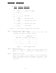
TABLE OF CONTENTS WARRANTY INFORMATION . . . . . . . . . . . . LIST OF FIGURES I. II. III. iii INTRODUCTION . . . . . . . . . . . . . . . . 1 BOARD DESCRIPTION . . . . . . . . . . . . . 1 16550 FUNCTIONAL DESCRIPTION . . . . . . . . 3 A. B. C. D. E. F. G. H. IV. . . . . . . . . . . . . . i INTERRUPT ENABLE REGISTER . . . . INTERRUPT IDENTIFICATION REGISTER FIFO CONTROL REGISTER . . . . . . LINE CONTROL REGISTER . . . . . . MODEM CONTROL REGISTER . . . . . LINE STATUS REGISTER . . . . . .
LIST OF FIGURES Figure Figure Figure Figure Figure Figure Figure Figure Figure Figure Figure Figure Figure Figure Figure Figure Figure Figure Figure Figure Figure 1. 2. 3. 4. 5. 6. 7. 8. 9. 10. 11. 12. 13. 14. 15. 16. 17. 18. 19. 20. 21. Figure 22. Figure 23. Figure 24. Figure 25. DS-2000 board layout . . . . . . . . 16550 internal registers . . . . . . Interrupt enable register . . . . . Interrupt identification register . Interrupt source identification . . FIFO control register . . . . . . .
I. INTRODUCTION The DS-2000 is a dual channel asynchronous serial communication adapter which utilizes balanced differential drivers and receivers to provide RS-422-A communications. It is capable of reliable communications over long distances (4000 feet) within noisy industrial environment. Data is communicated through two D-9 connectors which provide shielding from environmental noise.
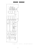
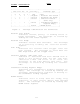
FUNCTIONAL Figure 1. iii DESCRIPTION DS-2000 board layout.
III. 16550 FUNCTIONAL DESCRIPTION FUNCTIONAL DESCRIPTION The 16550 is an upgrade of the standard 16450 Asynchronous Communications Element (ACE). Designed to be compatible with the 16450, the 16550 enters the character mode on reset and in this mode will appear as a 16450 to user software. An additional mode, FIFO mode, can be selected to reduce CPU overhead at high data rates.
FUNCTIONAL DESCRIPTION A . INTERRUPT D7 D6 D5 D4 D3 D2 D1 D0 +-------+ | 0 | +-------+ | 0 | +-------+ | 0 | +-------+ | 0 | +-------+ | EDSSI |----+-------+ | ELSI |----+-------+ | ETBEI |----+-------+ | ERBFI |----+-------+ Figure 3. ENABLE REGISTER MODEM status Receiver line status Transmitter holding register empty Received data available Interrupt enable register bit definitions.
FUNCTIONAL DESCRIPTION B . INTERRUPT IDENTIFICATION REGISTER +------+ | FFE |----- FIFO enable (FIFO only) +------+ D6 | 0 | +------+ D5 | 0 | +------+ D4 | 0 | +------+ D3 | IID2 |--+ +------+ | D2 | IID1 | +-- Interrupt identification +------+ | D1 | IID0 |--+ +------+ D0 | IP |----- Interrupt pending +------+ D7 Figure FFE 4. Interrupt definitions. identification bit - FIFO Enable: When logic 1, indicates FIFO mode enabled. IIDx - Interrupt Identification: Indicates highest priority any.
FUNC TIONAL DESCRIPTION +-------------------+----------+----------------------+ | IID2 IID1 IID0 IP | Priority | Interrupt Type | +-------------------+----------+----------------------+ | x x x 1 | N/A | None | | 0 1 1 0 | Highest | Receiver Line Status | | 0 1 0 0 | Second | Received Data Ready | | 1 1 0 0 | Second | Character Timeout | | | | (FIFO only) | | 0 0 1 0 | Third | Transmitter Holding | | | | Register Empty | | 0 0 0 0 | Fourth | MODEM Status | +-------------------+----------+-----------------
FUNCTIONAL DESCRIPTION C . FIFO CONTROL REGISTER +------+ | RXT1 |--+ +------+ +-D6 | RXT0 |--+ +------+ D5 | x |--+ +------+ +-D4 | x |--+ +------+ D3 | DMAM |----+------+ D2 | XRST |----+------+ D1 | RRST |----+------+ D0 | FE |----+------+ D7 Figure 6. Receiver trigger Reserved DMA mode select Transmit FIFO reset Receive FIFO reset FIFO enable FIFO control register bit definitions. RXTx - Receiver FIFO Trigger Level: Determines the trigger level interrupt as given in figure 7 below.
FUNCTIONAL DESCRIPTION RRST - Receive FIFO Reset: When set (logic 1), all bytes in the receiver FIFO are cleared and the counter is reset. The shift register is not cleared. RRST is selfclearing. FE - FIFO Enable: When set (logic 1), enables transmitter and receiver FIFOs. When cleared (logic 0), all bytes in both FIFOs are cleared. This bit must be set when other bits in the FIFO control register are written to or the bits will be ignored. D .
FUNCTIONAL DESCRIPTION STKP - Stick Parity: Forces parity to logic 1 or logic 0 if parity is enabled. See EPS, PEN, and figure 9. EPS - Even Parity Select: Selects even or odd parity if parity is enabled. See STKP, PEN, and figure 9. PEN - Parity Enable: Enables parity on transmission and verification on reception. See EPS, STKP, and figure 9.
FUNCTIONAL DESCRIPTION E . MODEM CONTROL +------+ | 0 | +------+ D6 | 0 | +------+ D5 | 0 | +------+ D4 | LOOP |----+------+ D3 | OUT2 |----+------+ D2 | OUT1 |----+------+ D1 | RTS |----+------+ D0 | DTR |----+------+ REGISTER D7 Figure 11. Loopback enable Output 2 Output 1 Request to send Data terminal ready MODEM control register bit definitions.
FUNCTIONAL F . LINE D7 D6 D5 D4 D3 D2 D1 D0 STATUS +------+ | FFRX |----+------+ | TEMT |----+------+ | THRE |----+------+ | BI |----+------+ | FE |----+------+ | PE |----+------+ | OE |----+------+ | DR |----+------+ Figure 12. DESCRIPTION REGISTER Error in FIFO RCVR (FIFO only) Transmitter empty Transmitter holding register empty Break interrupt Framing error Parity error Overrun error Data ready Line status register bit definitions. FFRX - FIFO Receiver Error: Always logic 0 in character mode.
FUNCTIONAL DESCRIPTION Bits BI, FE, PE, and OE are the sources of receiver line status interrupts. The bits are reset by reading the line status register. In FIFO mode, these bits are associated with a specific character in the FIFO and the exception is revealed only when that character reaches the top of the FIFO. BI - Break Interrupt: Indicates the receive data input has been in the spacing state (logic 0) for longer than one full word transmission time.
FUNCTIONAL G . MODEM STATUS DESCRIPTION REGISTER +------+ | DCD |----- Data carrier detect +------+ D6 | RI |----- Ring indicator +------+ D5 | DSR |----- Data set ready +------+ D4 | CTS |----- Clear to send +------+ D3 | DDCD |----- Delta data carrier detect +------+ D2 | TERI |----- Trailing edge ring indicator +------+ D1 | DDSR |----- Delta data set ready +------+ D0 | DCTS |----- Delta clear to send +------+ Figure 13. MODEM status register bit definitions.
FUNCTIONAL DESCRIPTION H . SCRATCHPAD REGISTER This register is not used by the 16550. used by the programmer for data storage. IV. FIFO INTERRUPT MODE It may be OPERATION 1. The receive data interrupt is issued when the FIFO reaches the trigger level. The interrupt is cleared as soon as the FIFO falls below the trigger level. 2. The interrupt identification register's receive data available indicator is set and cleared along with the receive data interrupt above. 3.
B AUD RATE SELECTION J1 +-----------+ 1| o o+ o |4 2| o o+ o |5 +-----------+ (a) ÷1 input clock J1 +-----------+ 1| o--o o |4 2| o o--o |5 +-----------+ (b) ÷2 input clock J1 +-----------+ 1| o o--o |4 2| o--o o |5 +-----------+ (c) ÷5 input clock J1 +-----------+ 1| o+ o--o |4 2| o+ o--o |5 +-----------+ (d) ÷10 input clock Figure The equation 14. Input clock frequency options. For compatibility, the jumper should be set at ÷10 ( 18.432 MHz ÷ 10 = 1.8432 MHz ).
ADDRESSING VI. ADDRESSING Each channel of the DS-2000 uses 8 consecutive I/O address locations. The base addresses are independent but must begin on an even 8-byte boundary (xxx0H - xxx7H or xxx8H - xxxFH). The numbers xxx are controlled by the Programmable Option Select (POS) and address decoders to provide complete 16-bit addressing for each channel. Sixteen choices of base address are provided for each channel and include the eight addresses defined as SERIAL 1 through SERIAL 8.
PROGRAMM ABLE OPTION SELECT The remaining POS registers are used for address and interrupt selections. These registers are programmed by the user through the IBM installation utility supplied with the PS/2. These registers are read/write but should not be written to by user software. The bit definitions of these registers are given in figures 16(a) and 16(b).
PROGRAMMABLE OPTION SELECT +-------------------------+-------------------+ | ADSx3 ADSx2 ADSx1 ADSx0 | Base address | +-------------------------+-------------------+ | 0 0 0 0 | 3F8H (Serial 1) | | 0 0 0 1 | 2F8H (Serial 2) | | 0 0 1 0 | 3220H (Serial 3) | | 0 0 1 1 | 3228H (Serial 4) | | 0 1 0 0 | 4220H (Serial 5) | | 0 1 0 1 | 4228H (Serial 6) | | 0 1 1 0 | 5220H (Serial 7) | | 0 1 1 1 | 5228H (Serial 8) | | 1 0 0 0 | 83F8H | | 1 0 0 1 | 82F8H | | 1 0 1 0 | B220H | | 1 0 1 1 | B228H | | 1 1 0 0 | C220H
OUT PUT CONFIGURATIONS IX. OUTPUT CONFIGURATIONS Two sets of jumpers are implemented on the DS-2000 to control the auxiliary driver/receiver set. Jumpers J2 and J3 perform identical functions on channels 1 and 2 respectively. The function of J2 and J3 is to control the source of the data exchanged on the auxiliary communication lines. The output sources are request to send (RTS), transmit clock (XCLK), and the auxiliary input (AUX IN). The inputs are clear to send (CTS) and receive clock (RCLK).
OUTPUT CONFIGURATIONS The other function of J2 and J3 is to configure the communication channel in half or full duplex mode. Half duplex operation is achieved by connecting pins 4 and 8 of the jumper block (figure 23). This allows the transmitter to be enabled and disabled using the data terminal ready (DTR) output in the modem control register. Full duplex operation is restored by removing the jumper on pins 4 and 8 (figures 21 and 22).
OUTPUT CONFIGURATIONS +-----------+ | RI +-+ +------+ | DCD +-+ +-+ inv. +-+ | DSR +-+ | +------+ | (4,5,6 for channel 1, | DTR +-+----+----o o o 1,2,3 for channel 2) | | J4 | +----------+ | RCLK +-----------+ | AUXIN | RS-422 +--- + | | +--+--+---------+ Receiver +--- | | 5 6| 7| 8| +----------+ | CTS +----o o+ o+ o+ Enable | RTS +----o o+ o+ o----------------+ | | 1 2| 3| 4 +----+---+ | | +--+-------------+ RS-422 +--- + | BAUDOUT +-----------+ AUXOUT | Driver +--- +-----------+ +--------+ Figure 19.
OUTPUT CONFIGURATIONS AUXIN ------+ +------ RCLK CTS --+ | | +-- DTR +-------------------+ 5 | o---o o+ o | 8 1 | o---o o+ o | 4 +-------------------+ RTS --+ | | +-- driver enable AUXOUT ------+ +------ XCLK J2 _ Channel 1 Figure 21.
EX TERNAL X. CONNECTIONS EXTERNAL CONNECTIONS Connections to peripheral equipment are made via a female D-9 connector. A pin-out of the D-9 connector and a detailed description of each output signal is illustrated in figures 24 and 25. Figure 24. D-9 output configuration.
INSTALLATION XI. INSTALLATION Make sure there is a copy of the original reference diskette available. This diskette must be modified to accept any option adapters. 1. Turn unit off. 2. Remove system cover as instructed in the IBM Quick Reference Guide. 3. Insert adapter into any vacant slot following the guidelines for installing an optional adapter in the IBM Quick Reference Guide. 4. Replace system cover. 5. Turn unit on and insert copy of reference diskette into drive A. 6.