EM78M611E Product Specification DOC. VERSION 1.1 ELAN MICROELECTRONICS CORP.
Trademark Acknowledgments: IBM is a registered trademark and PS/2 is a trademark of IBM. Windows is a trademark of Microsoft Corporation. ELAN and ELAN logo are trademarks of ELAN Microelectronics Corporation. Copyright © 2006 by ELAN Microelectronics Corporation All Rights Reserved Printed in Taiwan The contents of this specification are subject to change without further notice. ELAN Microelectronics assumes no responsibility concerning the accuracy, adequacy, or completeness of this specification.
Contents 1 2 3 4 5 6 7 8 General Description ................................................................................................ 1 Features ................................................................................................................... 1 Type Definition......................................................................................................... 3 Application.........................................................................................................
Contents 8.3 8.4 8.5 Extra Control Register..................................................................................... 21 USB Application FIFOs ................................................................................... 21 USB Application .............................................................................................. 22 8.5.1 8.5.2 8.6 Reset .............................................................................................................. 23 8.6.1 8.6.2 8.6.
EM78M611E Universal Serial Bus Series Microcontroller 1 General Description The EM78611E is a series of 8-bit Universal Serial Bus RISC architecture microcontroller, Multi-Time Programming (MTP) microcontrollers. It is specifically designed for USB low speed device application and to support standard devices such as PS/2 keyboard. The EM78611E also supports one device address and three endpoints.
EM78M611E Universal Serial Bus Series Microcontroller Built-in 8-bit RISC MCU 8-level stacks for subroutine nesting and interrupt 8-bit real time clock/counter (TCC) with overflow interrupt Six available interrupts Built-in RC oscillator free running for Watchdog Timer and Dual clock mode Two independent programmable prescalers for WDT and TCC Two power saving methods: 1. Power-down mode (Sleep mode) 2.
EM78M611E Universal Serial Bus Series Microcontroller Built-in 24-Channel Analog-to-Digital Converter (ADC) Up to 24 channels Up to 10 bits resolution 4 ADC conversion rates: 256K/128K/64K/32K Built-in 3.3V Voltage Regulator For MCU power supply Pull-up source for the external USB resistor on D-pin Package Type: 40-pin PDIP (600mil) (EM78M611EXAP) 44-pin QFP (10×10mm, footprint=3.
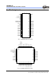
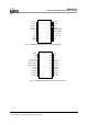
EM78M611E Universal Serial Bus Series Microcontroller 5 Pin Assignment VSS 1 40 OSCO V3.3 2 39 OSCI D+/CLK.
EM78M611E Universal Serial Bus Series Microcontroller P56/AD6 1 20 P55/AD5 P57/AD7 2 19 P54/AD4 P60/AD16 3 18 VNN P61/AD17 4 17 P94/VPP P62/AD18 5 16 P93/SE2/PWM2 P77 6 15 P92/SE1/PWM1 P76 7 14 D- / DATA /P75 VDD 8 13 D+ / CLK /P74 OSCI 9 12 V3.3 OSCO 10 11 VSS Fig. 3-3 EM78M611EXBP/BM/DM (20-Pin DIP/SOP/SSOP) OSCO 1 24 OSCI VSS 2 23 VDD V3.
EM78M611E Universal Serial Bus Series Microcontroller 6 Pin Description Symbol I/O P50 ~ P57 I/O General 8-bit bidirectional input/output port. All pins on this port can be internally pulled-high by software control. P60 ~ P67 I/O General 8-bit bidirectional input/output port. All pins on this port can be internally pulled-high by software control.
EM78M611E Universal Serial Bus Series Microcontroller 7 Block Diagram OSCI Built-in RC OSCO WDT Timer V3.3 3.
EM78M611E Universal Serial Bus Series Microcontroller 8 Function Description The EM78M611E memory is organized into three spaces, namely; User Program memory in 6K×13 bits ROM space, Data Memory in 144 bytes SRAM space, EEPROM space and USB Application FIFOs for EndPoint0, EndPoint1, and EndPoint2. Furthermore, several registers are used for special purposes. 8.1 Program Memory The program space of the EM78M611E is 6K words, and is divided into six pages. Each page is 1K words long.
EM78M611E Universal Serial Bus Series Microcontroller 8.2 Data Memory The Data Memory has 144 bytes SRAM space. It has also an on-chip USB Application FIFO space for USB Application. Figure 8-1 (next page) shows the organization of the Data Memory Space. 8.2.
EM78M611E Universal Serial Bus Series Microcontroller 8.2.2 Operation Registers The following subsections describe each of the Operation Registers of the Special Purpose Registers. The Operation Registers are arranged according to the order of the registers’ address. Note that some registers are read only, while others are both readable and writable. 8.2.2.1 R0 (Indirect Addressing Register) Default Value: (0B_0000_0000) R0 is not a physically implemented register.
EM78M611E Universal Serial Bus Series Microcontroller A12 A11 A10 A9 A8 Call Interrupt A7~A0 RET RETL RETI Stack 1 Stack 2 Stack 3 Stack 4 Stack 5 0000 Stack 6 Stack 7 Page 0 Stack 8 03FF 0400 Page 1 07FF 0800 Page 2 0BFF 1000 0000 : Reset Vector 0001 : Interrupt Vector Page 0 13FF 1400 Page 0 17FF 8.2.2.
EM78M611E Universal Serial Bus Series Microcontroller R3 [2] Zero flag. It will be set to 1 when the result of an arithmetic or logic operation is zero. R3 [3] Power down flag. It will be set to 1 during Power-on phase or by “WDTC” command and cleared when the MCU enters into Power down mode. It remains in its previous state after a Watchdog Reset. 0: Power down 1: Power-on R3 [4] Time-out flag. It will be set to 1 during Power-on phase or by “WDTC” command. It is reset to 0 by WDT time-out.
EM78M611E Universal Serial Bus Series Microcontroller 8.2.2.5 R4 (RAM Select Register) Default Value: (0B_00XX_XXXX) Bit 7 Bit 6 Bit 5 Bit 4 Bit 3 Bit 2 Bit 1 Bit 0 BK1 BK0 Ad5 Ad4 Ad3 Ad2 Ad1 Ad0 R4 (RAM select register) contains the address of the registers. R4 [0~5] used to select registers in 0x00h~0x3Fh. The address 0x00~0x1F is common space. After 0x1Fh, SRAM is divided into four banks, using Bank Select Register.
EM78M611E Universal Serial Bus Series Microcontroller 8.2.2.11 RA (EEPROM Control Register) Default Value: (0B_1111_1111) RA is a command register for EEPROM control. For detailed usage of this register, refer to Section 8.2.3 which describes the EEPROM embedded in the EM78M611E. 8.2.2.12 RB (Pattern Detect Application Control Register) Default Value: (0B_0000_0000) RB is a control register for controlling the Pattern Detect Application function.
EM78M611E Universal Serial Bus Series Microcontroller 8.2.2.12 RD (USB Application FIFO Address Register) Default Value: (0B_0000_0000) Bit 7 Bit 6 Bit 5 Bit 4 Bit 3 Bit 2 Bit 1 Bit 0 0 0 0 UAD4 UAD3 UAD2 UAD1 UAD0 RD [0~4] USB Application FIFO address registers. These five bits are the address pointers of USB Application FIFO. RD [5~7] Undefined registers. The default value is zero. 8.2.2.
EM78M611E Universal Serial Bus Series Microcontroller RF [2] USB Suspend interrupt flag. It will be set when the EM78M611E finds the USB Suspend Signal on USB bus. This bit is cleared by the firmware. RF [3] USB Reset interrupt flag. It will be set when the host issues the USB Reset signal. RF [4] P74/P75/P76/P77 Port state change interrupt flag. In PS2 Mode, only pins configured as inputs can cause this interrupt to occur.
EM78M611E Universal Serial Bus Series Microcontroller CONT (Control Register) Default Value: (0B_0011_1111) 8.2.3.2 Bit 7 Bit 6 Bit 5 Bit 4 Bit 3 Bit 2 Bit 1 Bit 0 LED INT TSR2 TSR1 TSR0 PSR2 PSR1 PSR0 Except for Bit 6 (Interrupt enable control bit), the CONT register can be read by the instruction "CONTR" and written by the instruction “CONTW". CONT [0~2] Watchdog Timer prescaler bits. These three bits are used as the Watchdog Timer prescaler. CONT [3~5] TCC Timer prescaler bits.
EM78M611E Universal Serial Bus Series Microcontroller 8.2.3.3 IOC5 ~IOC9 I/O (Port Direction Control Registers) Default Value: (0B_1111_1111) These are I/O port (Port 5 ~ Port 7) direction control registers. Each bit controls the I/O direction of three I/O ports respectively. When these bits are set to 1, the relative I/O pins become input pins. Similarly, the I/O pins becomes outputs when the relative control bits are cleared. 0 : Output direction 1 : Input direction 8.2.3.
EM78M611E Universal Serial Bus Series Microcontroller IOCA [6, 7] Select the operation frequency in Dual Clock Mode. Four frequencies are available and can be chosen as Dual Clock Mode in running the MCU program. 8.2.3.5 Dual_Frq.1 Dual_Frq.
EM78M611E Universal Serial Bus Series Microcontroller 8.2.3.8 IOCE (Special Function Control Register) Default Value: (0B_1101_0111) Bit 7 Bit 6 Bit 5 Bit 4 Bit 3 Bit 2 Bit 1 Bit 0 /Dual clock /WUE WTE RUN Device_Resume /PU8 /PU6 /PU5 IOCE [0, 1, 2] Port 5, Port 6, and Port 8 pull-high control bits. 0 : Enable 1 : Disable IOCE [3] Setting this bit will allow the UDC to execute resume signaling.
EM78M611E Universal Serial Bus Series Microcontroller 8.2.3.9 IOCF (Interrupt Mask Register) Default Value Bit 7 Bit 6 Bit 5 USB Host Resume_I E SE2_IE SE1_IE Bit 4 Bit 3 J (0B_0000_0000) Bit 2 Port7 state USB USB change_1E Reset_IE Suspend_IE Bit 1 Bit 0 EP0_IE TCC_IE IOCF [0~7] TCC / EP0 / USB Suspend / USB Reset / Port 7 State Change / SE1_IE / SE2_IE / USB Host Resume interrupt enable bits.
EM78M611E Universal Serial Bus Series Microcontroller Address (RD) 0X10 Data Byte Pointer of EP0 0X11 Data Byte Pointer of EP1 0X12 Data Byte Pointer of EP2 Counter 0X00 EP0's FIFO 0X01 EP1's FIFO 0X02 EP1's FIFO Pointer Counter Pointer Counter Pointer 0 0 0 1 1 1 2 2 2 3 3 3 4 4 4 5 5 5 6 6 6 7 7 7 Bi-directional Uni-directional Bi-directional 8.
EM78M611E Universal Serial Bus Series Microcontroller 8.5.2 Device Address and Endpoints EM78M611E supports one device address and three endpoints, EP0 for control endpoint, EP1 and EP2 for interrupt endpoint. Sending data to USB host in EM78M611E is very easy. Just write data into EP’s FIFO, then set flag, and the UDC will handle the rest. It will then confirm that the USB host has received the correct data from EM78M611E. 8.
EM78M611E Universal Serial Bus Series Microcontroller : // Set the Port 6 to input port MOV A, @0xFF IOW PORT6 // Read the state of Port 6 MOV PORT6, PORT6 // Clear the RUN bit IOR 0xE AND A, 0B11101111 IOW 0xE : : 8.7.2 Dual Clock Mode The EM78M611E has one internal oscillator for power saving application. Clearing the Bit IOCE [7] will enable the low frequency oscillator. At the same time, the external oscillator will be turned off.
EM78M611E Universal Serial Bus Series Microcontroller b) Signal from P.92 changes to high, and Pattern Counter value bigger than R10 register value. c) P.92 remains high, and the Pattern Counter value is equal to 0XFF. d) P.92 remains low, and the Pattern Counter value is equal to 0XFF.
EM78M611E Universal Serial Bus Series Microcontroller Pattern Detect Application (PDA) can calculate the length of one pattern and interrupt the MCU while the serial signal is transiting from high to low (or vise-versa). Then the MCU reads the length value from a specified register. 8.9.2 Control Register The PDA includes an enable control bit, one control register and 4-length counter registers in 0x10 ~0x13.
EM78M611E Universal Serial Bus Series Microcontroller high state, then the “high pattern counter“ will increase; otherwise the “low pattern counter” increases. As long as the signal state changes, the PDA will debounce signal and load the value of pattern counter into the respectively register for the firmware to read. For example, if the signal in P.92 is in “low” state, the low counter of P.92 will count continuously until the state of the input signal in P.92 changes.
EM78M611E Universal Serial Bus Series Microcontroller After the PDA function is enabled (by setting IOCA[2] to 1), user can write a default value to the High Pattern counter register and Low Pattern counter register. Then set the corresponding interrupt enable bit (IOCF[5]). When the counting value of one “H” pattern is bigger than the default value of R11, the Pattern Detecting interrupt will be generated.
EM78M611E Universal Serial Bus Series Microcontroller ERE [0~2] PWM Clock Prescaler PS2 PS1 PS0 Clock (Hz) Period/255 (s) 0 0 0 Fosc/3 0.5µ 0 0 1 Fosc/6 1µ 0 1 0 Fosc/12 2µ 0 1 1 Fosc/24 4µ 1 0 0 Fosc/48 8µ 1 0 1 Fosc/96 16µ 1 1 0 Fosc/192 32µ 1 1 1 Fosc/384 64µ ERE [6, 7] PWM1/PWM2 Enable Bit 0 : Disable 1 : Enable 8.11 Analog-To-Digital Converter (ADC) 8.11.
EM78M611E Universal Serial Bus Series Microcontroller ERA [0~4]: AD Channel Selector AD4 AD3 AD2 AD1 AD0 Channel I/O Port 0 0 0 0 0 0 P50 0 0 0 0 1 1 P51 0 0 0 1 0 2 P52 0 0 0 1 1 3 P53 0 0 1 0 0 4 P54 0 0 1 0 1 5 P55 0 0 1 1 0 6 P56 0 0 1 1 1 7 P57 0 1 0 0 0 8 P80 0 1 0 0 1 9 P81 0 1 0 1 0 10 P82 0 1 0 1 1 11 P83 0 1 1 0 0 12 P84 0 1 1 0 1 13 P85 0 1 1 1 0 14 P86 0 1 1 1 1 15 P87 1 0 0
EM78M611E Universal Serial Bus Series Microcontroller ERC (AD MSB Data Register) Default Value: (0B_0000_0000) Bit 7 Bit 6 Bit 5 Bit 4 Bit 3 Bit 2 Bit 1 Bit 0 Bit 9 Bit 8 Bit 7 Bit 6 Bit 5 Bit 4 Bit 3 Bit 2 2 bits AD MSB Digital Data. ERD (AD Control Register) Default Value: (0B_0000_0000) Bit 7 Bit 6 Bit 5 Bit 4 Bit 3 Bit 2 Bit 1 Bit 0 0 0 0 0 0 - ADPS1 ADPS0 ERD [0 1]: The clock source of AD converting time. 00: 256kHz 01: 128kHz 10: 64kHz 11: 32kHz 8.
EM78M611E Universal Serial Bus Series Microcontroller 9 Absolute Maximum Ratings Symbol Min Temperature under bias Max Unit 0 70 ºC Storage temperature -65 150 ºC Input voltage -0.5 6.0 V Output voltage -0.5 6.0 V Min Type Max 10 DC Electrical Characteristic T = 25ºC, VDD=5V, VSS=0V Symbol Parameter Condition Unit 3.3V Regulator VRag Output voltage of 3.3V Regulator VResetL Low Power Reset detecting low Voltage VResetH Low Power Reset detecting high Voltage Ireg 3.
EM78M611E Universal Serial Bus Series Microcontroller Symbol Parameter Condition Min Type Max Unit IOH2 Output High Voltage (P74, P75) ISink = 5.0mA VDD = 5V − 5 − mA IOH3 Output High Voltage (Port 5 & Port 6 & Port 8 and P90~P93, P95, P96) ISink = 10.0mA VREG = 3.3V − 10 − mA IOL1 Output Low Voltage (P76 and P77 normal mode) ISink = 10.0mA VDD = 5V − 10 − mA IOL2 Output Low Voltage (P74, P75) ISink = 10.0mA VDD = 5V − 5 − mA IOL3 Output Low Voltage ISink = 10.
EM78M611E Universal Serial Bus Series Microcontroller 11 Application Circuit NOTE A. BC1 , BC2 : load Capacitor B. C1 (bypass capacitor) : that placed adjacent to VDD pin , to minimize noise. C. C2 , C3 (power capacitor) : that placed adjacent to the Power source , will improve transient response and ripple rejection. 34 • Product Specification (V1.1) 11.22.
EM78M611E Universal Serial Bus Series Microcontroller APPENDIX A Special Register Map Operation Registers Address Name Bit 7 Bit 6 Bit 5 Bit 4 Bit 3 Bit 2 Bit1 Bit 0 Default Value 0x00 R0 Indirect Addressing Register 0B_0000_0000 0x01 R1 (TCC) Timer/Clock Counter 0B_0000_0000 0x02 R2 (PC) Program Counter 0B_0000_0000 0x03 R3 (STATUS) PS2 PS1 PS0 0x04 R4 (RSR) BK1 BK0 Select the register( Address: 00~3F) in indirect addressing mode 0x05 R5 (Port 5) P57 P56 P55 P54 P53
EM78M611E Universal Serial Bus Series Microcontroller Control Registers Address Name CONT Bit 7 S7 Bit 6 INT Bit 5 TSR2 Bit 4 Bit 3 SR1 Bit 2 TSR0 PSR2 Bit 1 Bit 0 Default Value PSR1 PSR0 0B_0011_1111 0x05 IOC5 Port 5 Direction Control Register 0B_1111_1111 0x06 IOC6 Port 6 Direction Control Register 0B_1111_1111 0x07 IOC7 Port 7 Direction Control Register 0B_1111_1111 0x08 IOC8 Port 8 Direction Control Register 0B_1111_1111 0x09 IOC9 Port 9 Direction Control Register 0
EM78M611E Universal Serial Bus Series Microcontroller B Instruction Set Each instruction in the instruction set is a 13-bit word divided into an OP code and one or more operands. All instructions are executed within one single instruction cycle (consisting of two oscillator periods), unless the program counter is changed by(a) Executing the instruction "MOV R2, A", "ADD R2,A", "TBL", or any other instructions that write to R2 (e.g. "SUB R2,A", "BS R2,6", "CLR R2", ⋅⋅⋅⋅).
EM78M611E Universal Serial Bus Series Microcontroller Binary Instruction Hex Mnemonic Operation Status Affected 0 0001 10rr rrrr 01rr DECA R R-1 → A Z 0 0001 11rr rrrr 01rr DEC R R-1 → R Z 0 0010 00rr rrrr 02rr OR A,R A ∨ VR → A Z 0 0010 01rr rrrr 02rr OR R,A A ∨ VR → R Z 0 0010 10rr rrrr 02rr AND A,R A&R→A Z 0 0010 11rr rrrr 02rr AND R,A A&R→R Z 0 0011 00rr rrrr 03rr XOR A,R A⊕R→A Z 0 0011 01rr rrrr 03rr XOR R,A A⊕R→R Z 0 0011 10rr rrrr 03rr ADD A,R A+R→A
EM78M611E Universal Serial Bus Series Microcontroller C Code Option Register EM78M611E has two Code option registers, which are not part of the normal program memory. The option bits cannot be accessed during normal program execution. Address 000: Bit 12 11 10 9 8 7 6 5 4 3 2 1 0 Mnemonic ID_8 ID_7 ID_6 ID_5 ID_4 ID_3 ID_2 ID_1 ID_0 OST_1 OST_0 Frequency /Protect Address 001: Bit 5 4 3 2 1 0 Mnemonic /AD_Hold /R.S.
EM78M611E Universal Serial Bus Series Microcontroller Bit 4 (/R.S.