EM78P468N/L 8-Bit Microcontroller Product Specification DOC. VERSION 1.5 ELAN MICROELECTRONICS CORP.
Trademark Acknowledgments: IBM is a registered trademark and PS/2 is a trademark of IBM. Windows is a trademark of Microsoft Corporation. ELAN and ELAN logo are trademarks of ELAN Microelectronics Corporation. Copyright © 2004~2007 by ELAN Microelectronics Corporation All Rights Reserved Printed in Taiwan, ROC The contents of in this specification are subject to change without notice. ELAN Microelectronics assumes no responsibility concerning the accuracy, adequacy, or completeness of this specification.
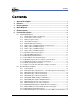
Contents Contents 1 2 3 4 5 6 General Description ······················································································ 1 Features ········································································································· 1 Pin Assignment ····························································································· 2 Block Diagram ······························································································· 3 Pin Description················
Contents 6.2.14 6.2.15 6.2.16 6.2.17 6.2.18 6.2.19 6.2.20 6.2.21 IOC71/TCCCR (TCC Control Register)............................................................ 19 IOC81/WDTCR (WDT Control Register) .......................................................... 20 IOC91/CNT12CR (Counters 1, 2 Control Register) ......................................... 20 IOCA1/HLPWTCR (High/Low Pulse Width Timer Control Register) ................ 21 IOCB1/P6PH (Port 6 Pull-high Control Register) ...............................
Contents APPENDIX A B C D E Package Type ······························································································ 67 Package Information··················································································· 68 EM78P468L Program Pin List····································································· 71 ICE 468XA ···································································································· 72 Quality Assurance and Reliability···················
Contents vi • Product Specification (V1.5) 01.15.
EM78P468N/EM78P468L 8-Bit Microcontroller 1 General Description The EM78P468N/L is an 8-bit microprocessor designed and developed with low-power and high-speed CMOS technology. Integrated onto a single chip are on chip Watchdog Timer (WDT), Data RAM, ROM, programmable real time clock counter, internal/external interrupt, power down mode, LCD driver, infrared transmitter function, and tri-state I/O. The series has an on-chip 4K×13-bit Electrical One Time Programmable Read Only Memory (OTP-ROM).
EM78P468N/EM78P468L 8-Bit Microcontroller 4 2 4 1 4 0 3 9 3 8 3 7 3 6 P5.5/INT1 4 3 NC 4 4 P5.6/TCC 4 5 P6.0 4 6 NC 4 7 P5.7/IROUT 4 8 P6.1 3 3 P6.2 3 4 P6.3 3 5 P6.4 3 6 P6.5 3 7 P6.7 3 8 P6.6 3 9 NC 4 0 P5.5/INT1 4 1 NC 4 2 P5.6/TCC P6.1 4 3 P6.0 P6.2 4 4 NC P6.3 4 5 P5.7/IROUT P6.4 4 6 P6.7 4 7 P6.5 4 8 P6.6 NC 4 9 NC NC 5 0 SEG31/P8.7 SEG30/P8.6 5 1 64-Pin LQFP SEG31/P8.7 (2) 64-Pin QFP SEG29/P8.
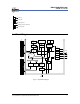
EM78P468N/EM78P468L 8-Bit Microcontroller Input Pin Output Pin Input/Output Pin Digital I/O Pin/LCD Output Pin LCD Output Pin 4 Block Diagram P8 P80 P81 P82 P83 P84 P85 P86 P87 ROM PC Instruction Register 8-level stack (13-bit) Crystal Oscillation Generation P7 P70 P71 P72 P73 P74 P75 P76 P77 RC PLL Instruction Decoder Rese t LCD WDT PWM1/IR (Timer 1,2) Mux. TCC ALU CNTR 1 TCC CNTR1 CNTR2 P6 P60 P61 P62 P63 P64 P65 P66 P67 PWM CNTR 2 R4 RAM ACC R3 (Status Reg.
EM78P468N/EM78P468L 8-Bit Microcontroller 5 Pin Description Table 1 (a) Pin Description for Package of QFP64 and LQFP64 Symbol 4• Pin No. Type Function 1-bit General purpose input/output pin/external interrupt. INT0 interrupt source can be set to falling or rising edge by IOC71 register Bit 7 (INT_EDGE). Wakes up from sleep mode and idle mode when the pin status changes. 1-bit General purpose input/output pin/external interrupt. Interrupt source is a falling edge signal.
EM78P468N/EM78P468L 8-Bit Microcontroller Table 2 (b) Pin Description for Package of QFP44 and LQFP44 Symbol Pin No. Type P5.4/INT0 21 I/O P5.5/INT1 22 I/O P5.6/TCC 23 I/O P5.7/IROUT 24 I/O 25~32 I/O COM3~0 6~9 O SEG11~SEG14 5~2 O SEG16/P7.0 SEG17/P7.1 ~ SEG23/P7.7 1 44 ~ 38 O/(I/O) SEG24/P8.0 ~ SEG31/P8.4 37 ~ 33 O/(I/O) VB 10 O VA 11 O VLCD2 12 O VLCD3 13 O /RESET 14 I P6.0~P6.7 Function 1-bit General purpose input/output pin/external interrupt.
EM78P468N/EM78P468L 8-Bit Microcontroller 6 Function Description 6.1 Operational Registers 6.1.1 R0/IAR (Indirect Addressing Register) (Address: 00h) R0 is not a physically implemented register. Its major function is to perform as an indirect address pointer. Any instruction using R0 as a register, actually accesses the data pointed by the RAM Select Register (R4). 6.1.
EM78P468N/EM78P468L 8-Bit Microcontroller R3 PC A11 00 PAGE0 0000~03FF 01 PAGE1 0400~07FF A10 A9 A8 CALL RET RETL RETI 10 PAGE2 0800~0BFF A7 ~ STACK LEVEL 1 STACK LEVEL 2 STACK LEVEL 4 STACK LEVEL 5 STACK LEVEL 6 Reset v ector 000H TCC ov erf low interrupt v ector 003H Exteral INT0 pin interrupt v ector 006H Exteral INT1 pin interrupt v ector 009H Counter 1 underf low interrupt v ector 00CH Counter 2 underf low interrupt v ector 00FH high pulse width timer underf low interrupt v ector
EM78P468N/EM78P468L 8-Bit Microcontroller 6.1.4 R3/SR (Status Register) (Address: 03h) Bit 7 Bit 6 Bit 5 Bit 4 Bit 3 Bit 2 Bit 1 Bit 0 − PS1 PS0 T P Z DC C Bit 7: Not used Bits 6 ~ 5 (PS1 ~ 0): Page select bits PS1 PS0 ROM Page (Address) 0 0 Page 0 (000H ~ 3FFH) 0 1 Page 1 (400H ~ 7FFH) 1 0 Page 2 (800H ~ BFFH) 1 1 Page 3 (C00H ~ FFFH) PS0~PS1 are used to select a ROM page. User can use the PAGE instruction (e.g. PAGE 1) or set PS1~PS0 bits to change the ROM page.
EM78P468N/EM78P468L 8-Bit Microcontroller 6.1.5 R4/RSR (RAM Select Register) (Address: 04h) Bit 7 Bit 6 Bit 5 Bit 4 Bit 3 Bit 2 Bit 1 Bit 0 RBS1 RBS0 RSR5 RSR4 RSR3 RSR2 RSR1 RSR0 Bits 7 ~ 6 (RBS1 ~ RBS0): determine which bank is activated among the four banks. See the data memory configuration in Fig. 6-2. Use the BANK instruction (e.g. BABK 1) to change banks. Bits 5 ~ 0 (RSR5 ~ RSR0): used to select up to 64 registers (Address: 00~3F) in indirect addressing mode.
EM78P468N/EM78P468L 8-Bit Microcontroller 6.1.9 R8/Port 8 (Port 8 I/O Data Register) (Address: 08h) Bit 7 Bit 6 Bit 5 Bit 4 Bit 3 Bit 2 Bit 1 Bit 0 R87 R86 R85 R84 R83 R82 R81 R80 Bits 7~0: 8-bit I/O registers of Port 8 User can use IOC80 register to define each bit either as input or output. 6.1.
EM78P468N/EM78P468L 8-Bit Microcontroller 6.1.
EM78P468N/EM78P468L 8-Bit Microcontroller Bit 1 (CNT2EN): Counter 2 enable bit CNT2EN = “0” : Disable Counter 2. Stop counting operation. CNT2EN = “1” : Enable Counter 2. Start counting operation. Bit 0 (CNT1EN): Counter 1 enable bit CNT1EN = “0” : Disable Counter 1. Stop counting operation. CNT1EN = “1” : Enable Counter 1. Start counting operation. 6.1.
EM78P468N/EM78P468L 8-Bit Microcontroller CPU Operation Mode Code option HLFS=1 Normal Mode Code option HLFS=0 fm:oscillation fs: oscillation it must delay a little times for the main oscillation stable w hile your system timing control is conscientious RESET CPU: using fosc CPUS="0" CPUS="1" SLEEP Mode IDLE="0" SLEP IDLE="1" SLEP Green Mode Fm:stop Fs: stop fm:stop fs:oscillation CPU: stop CPU: using fs Wake up IDLE Mode fm:stop fs:oscillation w ake up CPU: stop The w ake up time from i
EM78P468N/EM78P468L 8-Bit Microcontroller Bit 4: Not used Bit 3 (IROUTE): Define the function of P5.7/IROUT pin. IROUTE = “0” : for bi-directional general I/O pin. IROUTE = “1” : for IR or PWM output pin, the control bit of P5.7 (Bit 7 of IOC50) must be set to “0” Bit 2 (TCCE): Define the function of P5.6/TCC pin. TCCE = “0” : for bi-directional general I/O pin. TCCE = “1” : for external input pin of TCC, the control bit of P5.6 (Bit 6 of IOC50) must be set to “1” Bit 1 (EINT1): Define the function of P5.
EM78P468N/EM78P468L 8-Bit Microcontroller 6.2 Special Purpose Registers 6.2.1 A (Accumulator) Internal data transfer operation, or instruction operand holding usually involves the temporary storage function of the Accumulator, which is not an addressable register. Registers of IOC Page 0 (IOC50 ~ IOCF0, Bit 0 of R5 = “0”) 6.2.
EM78P468N/EM78P468L 8-Bit Microcontroller 6.2.3 IOC60/P6CR (Port 6 I/O Control Register) (Address: 06h, Bit 0 of R5 = “0”) Bit 7 Bit 6 Bit 5 Bit 4 Bit 3 Bit 2 Bit 1 Bit 0 IOC67 IOC66 IOC65 IOC64 IOC63 IOC62 IOC61 IOC60 Bit 7 (IOC67) ~ Bit 0(IOC60): Port 6 I/O direction control register IOC6x =”0”: set the relative Port 6.x I/O pins as output IOC6x =”1”: set the relative Port 6.x I/O pin into high impedance (input pin) 6.2.
EM78P468N/EM78P468L 8-Bit Microcontroller 6.2.8 IOCB0/CNT1PR (Counter 1 Preset Register) (Address: 0Bh, Bit 0 of R5 = “0”) Bit 7 Bit 6 Bit 5 Bit 4 Bit 3 Bit 2 Bit 1 Bit 0 Bit 7 Bit 6 Bit 5 Bit 4 Bit 3 Bit 2 Bit 1 Bit 0 Bit 7 ~ Bit 0: These are Counter 1 buffers which user can read and write. Counter 1 is an 8-bit down-count timer with 8-bit prescaler used to preset the counter and read the preset value. The prescaler is set by the IOC91 register.
EM78P468N/EM78P468L 8-Bit Microcontroller 6.2.11 IOCE0/LPWTPR (Low-Pulse Width Timer Preset Register) (Address: 0Eh, Bit 0 of R5 = “0”) Bit 7 Bit 6 Bit 5 Bit 4 Bit 3 Bit 2 Bit 1 Bit 0 Bit 7 Bit 6 Bit 5 Bit 4 Bit 3 Bit 2 Bit 1 Bit 0 Bit 7 ~ Bit 0: All are low-pulse width timer buffer that user can read and write. Low-pulse width timer preset is an eight-bit down-counter with 8-bit prescaler that is used as IOCE0 to preset the counter and read preset value.
EM78P468N/EM78P468L 8-Bit Microcontroller Bit 2 (/WUE8L): 0/1 → enable/disable P8.0~P8.3 pin change wake-up function Bit 1 (/WUE6H): 0/1 → enable/disable P6.4~P6.7 pin change wake-up function Bit 0 (/WUE6L): 0/1 → enable/disable P6.0~P6.3 pin change wake-up function * Port 6 and Port 8 must not be set as input floating when wake-up function is enabled. “Enable” is the initial state of wake-up function. 6.2.
EM78P468N/EM78P468L 8-Bit Microcontroller 6.2.15 IOC81/WDTCR (WDT Control Register) (Address: 08h, Bit 0 of R5 = “1”) Bit 7 Bit 6 Bit 5 Bit 4 Bit 3 Bit 2 Bit 1 Bit 0 − − − − WDTE WDTP2 WDTP1 WDTP0 Bits 7 ~ 4: Not used Bit 3 (WDTE): Watchdog timer enable. This control bit is used to enable the Watchdog timer, WDTE = “0”: Disable WDT function WDTE = “1”: enable WDT function Bits 2 ~ 0 (WDTP2 ~ WDTP0): Watchdog Timer prescaler bits. The WDT clock source is sub-oscillation frequency.
EM78P468N/EM78P468L 8-Bit Microcontroller Bit 3 (CNT1S): Counter 1 clock source select 0/1 → Fs/ Fm* Bits 2~0 (CNT1P2 ~ CNT1P20): Counter 1 prescaler select bits CNT1P2 CNT1P1 CNT1P0 0 0 0 Counter 1 Scale 1:2 0 0 1 1:4 0 1 0 1:8 0 1 1 1:16 1 0 0 1:32 1 0 1 1:64 1 1 0 1:128 1 1 1 1:256 6.2.
EM78P468N/EM78P468L 8-Bit Microcontroller 6.2.18 IOCB1/P6PH (Port 6 Pull-high Control Register) (Address: 0Bh, Bit 0 of R5 = “1”) Bit 7 Bit 6 Bit 5 Bit 4 Bit 3 Bit 2 Bit 1 Bit 0 PH67 PH66 PH65 PH64 PH63 PH62 PH61 PH60 Bit 7 ~ Bit 0 (PH67 ~ PH60): The enable bits of Port 6 pull high function. PH6x = “0”: disable pin of P6.x internal pull-high resistor function PH6x = “1”: enable pin of P6.x internal pull-high resistor function 6.2.
EM78P468N/EM78P468L 8-Bit Microcontroller 6.3 TCC and WDT Prescaler Two 8-bit counters are available as prescalers for the TCC (Time Clock Counter) and WDT (Watchdog Timer). The TCCP2~TCCP0 bits of the IOC71 register are used to determine the ratio of the TCC prescaler. Likewise, the WDTP2~WDTP0 bits of the IOC81 register are used to determine the WDT prescaler.
EM78P468N/EM78P468L 8-Bit Microcontroller WDT Setting Flowchart START N Use WDT function ? Y Enable WDT function : set bit 7 of Code option Word 0 to "0" Setting WDT prescaler (IOC81 register) Disable WDT function : set bit 7 of Code option Word 0 to "1" WDTtime= prescaler*256/Fs Fs: sub-oscillator frequency Enable WDT (bit 3 of IOC81) END TCC Setting Flowchart START from External Input from Instruction Cycle TCC clock source? External/ instruction cycle *set clock source from external TCC pin (s
EM78P468N/EM78P468L 8-Bit Microcontroller 6.4 I/O Ports The I/O registers, (Port 5, Port 6, Port 7 and Port 8), are bi-directional tri-state I/O ports. Port 6 and Port 8 are pulled-high internally by software; Port 6 is also pulled-low internally by software. Furthermore, Port 6 has its open-drain output also through software. Port 6 and Port 8 features an input status changed interrupt (or wake-up) function and is pulled-high by software.
EM78P468N/EM78P468L 8-Bit Microcontroller Table 2 Summary of Registers Initialized Values Address 0x05 0x06 0x07 0x08 0x09 0x0A 0x0B 0x0C 0x0D 0x0E 0x0F 0x06 26 • Name Reset Type Bit 7 Bit 6 Bit Name IOC57 IOC56 Power-on 1 1 IOC50 /RESET & WDT 1 1 (P5CR) Wake-up from P P Pin Change Bit Name IOC67 IOC66 Power-on 1 1 IOC60 /RESET & WDT 1 1 (P6CR) Wake-up from P P Pin Change Bit Name IOC77 IOC76 Power-on 1 1 IOC70 /RESET & WDT 1 1 (P7CR) Wake-up from P P Pin Change Bit Name IOC87 IOC86 Power
EM78P468N/EM78P468L 8-Bit Microcontroller Address 0x07 0x08 0x09 0x0A 0x0B 0x0C 0x0D 0x0E 0x00 0x01 0x02 0x03 0x04 Name Reset Type Bit Name Power-on IOC71 (TCCCR) /RESET & WDT Wake-up from Pin Change Bit Name Power-on IOC81 (WDTCR) /RESET &WDT Wake-up from Pin Change Bit Name Power-on IOC91 /RESET & WDT (CNT12CR) Wake-up from Pin Change Bit Name Power-on IOCA1 /RESET & WDT (HLPWTCR) Wake-up from Pin Change Bit Name Power-on IOCB1 /RESET & WDT (P6PH) Wake-up from Pin Change Bit Name Power-on
EM78P468N/EM78P468L 8-Bit Microcontroller Address 0x05 0x06 0x7 0x8 0x9 0xA 0xB 0xC 0xD 0xE 0xF 0x10 ~ 0x3F Name Reset Type Bit Name Power-on /RESET & WDT Wake-up from Pin Change Bit Name Power-on R6 /RESET & WDT (Port 6) Wake-up from Pin Change Bit Name Power-on R7 /RESET & WDT (Port 7) Wake-up from Pin Change Bit Name Power-on R8 /RESET & WDT (Port 8) Wake-up from Pin Change Bit Name Power-on R9 /RESET & WDT (LCDCR) Wake-up from Pin Change Bit Name Power-on RA /RESET & WDT (LCD_ADDR) Wake-
EM78P468N/EM78P468L 8-Bit Microcontroller The controller can be awakened from sleep mode and idle mode.
EM78P468N/EM78P468L 8-Bit Microcontroller 6.6 Oscillator 6.6.1 Oscillator Modes The EM78P468N/EM78P468L can operate in three different oscillator modes i.e., a.) Main oscillator (R-OSCI, OSCO), such as RC oscillator with external resistor and Internal capacitor mode (ERIC); b.) Crystal oscillator mode; and c.) PLL operation mode (R-OSCI connected to 0.01μF capacitor to Ground). User can select which mode by programming FMMD1 and FMMD0 in the Code Options Register.
EM78P468N/EM78P468L 8-Bit Microcontroller Bits 6~4 (CLK2~0) of RD: main clock selection bits for PLL mode (code option select) 6.6.3 CLK2 CLK1 CLK0 0 0 0 0 0 1 Fs×130 Fs×65 Main clock Example Fs=32.768KHz 4.26 MHz 2.13 MHz 0 1 0 Fs×65/2 1.065 MHz 0 1 1 Fs×65/4 532 kHz 1 × × Fs×244 8 MHz Crystal Oscillator/Ceramic Resonators (Crystal) This LSI can be driven by an external clock signal through the R-OSCI pin as shown in Fig.6-7 below.
EM78P468N/EM78P468L 8-Bit Microcontroller 6.6.4 RC Oscillator Mode with Internal Capacitor If both precision and cost are taken into consideration, this LSI also offers a special oscillation mode, which has an on-chip internal capacitor and an external resistor connected to VDD. The internal capacitor functions as temperature compensator. In order to obtain more accurate frequency, a precise resistor is recommended. VDD Rext R-OSCI or Xin EM78P468N Fig.
EM78P468N/EM78P468L 8-Bit Microcontroller 6.7.1 External Power-on Reset Circuit This circuit implements an external RC to produce a reset pulse (see Fig. 6-10). The pulse width (time constant) should be kept long enough to allow VDD to reach minimum operation voltage. This circuit is used when the power supply rise time is slow. Because the current leakage from the /RESET pin is ±5μA, it is recommended that R should not be greater than 40K. In this way, the voltage at Pin /RESET is held below 0.2V.
EM78P468N/EM78P468L 8-Bit Microcontroller 6.8 Interrupt This LSI has eight interrupt sources as listed below: TCC overflow interrupt. External interrupt P5.4/INT0 pin External interrupt P5.
EM78P468N/EM78P468L 8-Bit Microcontroller Table 3 Interrupt Vector Interrupt Vector Interrupt Status 0003H TCC overflow interrupt. 0006H External interrupt P5.4/INT0 pin 0009H External interrupt P5.5/INT1 pin 000CH Counter 1 underflow interrupt 000FH Counter 2 underflow interrupt 0012H High-pulse width timer underflow interrupt 0015H Low-pulse width timer underflow interrupt 0018H Port 6, Port 8 input status change wake up 6.
EM78P468N/EM78P468L 8-Bit Microcontroller When the LCD function is disabled, all common/segment output is set to ground (GND) level Bit 3: Not used Bit 2 (LCDTYPE): LCD drive waveform type select bit LCDTYPE = “0”: “A” type waveform LCDTYPE = “1”: “B” type waveform Bits 1 ~ 0 (LCDF1 ~ LCDF0): LCD frame frequency control bits LCDF1 LCDF0 0 LCD Frame Frequency (e.g. Fs=32.768kHz) 1/2 Duty 1/3 Duty 1/4 Duty 0 Fs/(256×2)=64.0 Fs/(172×3)=63.5 Fs/(128×4)=64.0 0 1 Fs/(280×2)=58.5 Fs/(188×3)=58.
EM78P468N/EM78P468L 8-Bit Microcontroller 6.9.
EM78P468N/EM78P468L 8-Bit Microcontroller Boosting circuits connection for LCD voltage VDD VLCD2(2*VDD/3) VA VB VLCD3(1*VDD/3) GND External circuit for 1/3 Bias VDD VLCD2(VDD/2) VA VB VLCD3(VDD/2) GND External circuit for 1/2 Bias Fig. 6-15 Charge Bump Circuit Connection (Cext=0.1μf ) 38 • Product Specification (V1.5) 02.15.
EM78P468N/EM78P468L 8-Bit Microcontroller 1 frame 1 frame VDD VLCD2,3 COM 0 VDD VLCD2,3 COM 0 GND GND VDD VLCD2,3 COM 1 VDD VLCD2,3 COM 1 GND GND VDD VLCD2,3 SEG N VDD VLCD2,3 SEG N GND GND VDD VDD VLCD2,3 GND SEG N - COM0 ON -VLCD2,3 VLCD2,3 GND SEG N - COM0 ON -VLCD2,3 -VDD -VDD VDD VDD VLCD2,3 SEG N - COM1 VLCD2,3 SEG N - COM1 GND OFF GND OFF -VLCD2,3 1/2 bias, 1/2 duty A type -VLCD2,3 -VDD 1/2 bias, 1/2 duty B type -VDD Fig.
EM78P468N/EM78P468L 8-Bit Microcontroller 1 frame 1 frame VDD VDD VLCD2 VLCD2 COM 0 COM 0 VLCD3 VLCD3 GND GND VDD VDD VLCD2 VLCD2 COM 1 COM 1 VLCD3 VLCD3 GND GND VDD VDD VLCD2 COM 2 VLCD2 COM 2 VLCD3 VLCD3 GND GND VDD VDD VLCD2 VLCD2 SEG N SEG N VLCD3 VLCD3 GND GND VDD VDD VLCD3 SEG N - COM0 VLCD3 SEG N - COM0 GND GND ON ON -VLCD3 -VLCD3 -VDD -VDD VDD VDD VLCD3 SEG N - COM1 VLCD3 SEG N - COM1 GND GND OFF OFF -VLCD3 -VLCD3 1/3 bias, 1/3 duty A typ
EM78P468N/EM78P468L 8-Bit Microcontroller 6.10 Infrared Remote Control Application/PWM Waveform Generate This LSI can output infrared carrier in user-friendly or in PWM standard waveform. The IR and PWM waveform generated functions include an 8-bit down count timer/counter, high-pulse width timer, low-pulse width timer, and IR control register. The IR system block diagram is shown in Fig. 6-20.
EM78P468N/EM78P468L 8-Bit Microcontroller The IROUT output waveform is further explained in the following figures: Fig. 6-21 LGP=0, HF=1, the IROUT waveform can modulate Fcarrier waveform when in low-pulse width time. Fig. 6-22 LGP=0, HF=0, the IROUT waveform cannot modulate Fcarrier waveform when in low-pulse width time. So IROUT waveform is determined by high-pulse time and low-pulse time. This mode can produce standard PWM waveform. Fig.
EM78P468N/EM78P468L 8-Bit Microcontroller Fcarrier low-pulse width high-pulse width low-pulse width high-pulse width HF start IRE IR disable IROUT Always high-level Fig. 6-23 LGP=0, IROUT Pin Output Waveform Fcarrier low-pulse width high-pulse width low-pulse width high-pulse width HF start IRE IR disable IROUT Always high-level Fig.
EM78P468N/EM78P468L 8-Bit Microcontroller IR/PWM Function Enable Flowchart Start Start SET P5.7 to Output state (IOC 50) SET P5.7 for IR/PWM Function Output Pin (RE) SET P5.7 to Output state (IOC 50) SET P5.
EM78P468N/EM78P468L 8-Bit Microcontroller 6.11 Code Options The EM78P468N/L has one Code Option word that is not a part of the normal program memory. The option bits cannot be accessed during normal program execution. Code Option Register and Customer ID Register arrangement distribution: Word 1 of code options is for customer ID code application. Word 1 Bit 12~Bit 0 Word 0 of Code Options is for IC function setting.
EM78P468N/EM78P468L 8-Bit Microcontroller Bit 3 (HLP): Power consumption selection. If the system usually runs in green mode, it must be set to low power consumption to help support the energy saving issue. It is recommended that low power consumption mode is selected. HLP = “0”: Low power consumption mode HLP = “1”: High power consumption mode Bits 2~0 (PR2~PR0): Protect Bit PR2~PR0 are protection bits. Each protect status is as follows: 6.
EM78P468N/EM78P468L 8-Bit Microcontroller Convention: R = Register designator that specifies which one of the registers (including operation and general purpose registers) is to be utilized by the instruction. b = Bit field designator that selects the value for the bit located in the register R and which affects the operation.
EM78P468N/EM78P468L 8-Bit Microcontroller Binary Instruction Hex Mnemonic Operation 0 0110 00rr rrrr 06rr RRCA R 0 0110 01rr rrrr 06rr RRC R 0 0110 10rr rrrr 06rr RLCA R 0 0110 11rr rrrr 06rr RLC R 0 0111 00rr rrrr 07rr SWAPA R 0 0 0 0 0 0 0 0111 0111 0111 100b 101b 110b 111b 01rr 10rr 11rr bbrr bbrr bbrr bbrr rrrr rrrr rrrr rrrr rrrr rrrr rrrr 07rr 07rr 07rr 0xxx 0xxx 0xxx 0xxx SWAP JZA JZ BC BS JBC JBS R R R R, R, R, R, 1 00kk kkkk kkkk 1kkk CALL k 1 1 1
EM78P468N/EM78P468L 8-Bit Microcontroller 6.13 Timing Diagram AC Test Input/Output Waveform 2.4 2.0 0.8 TEST POINTS 2.0 0.8 0.4 AC Testing : Input is driven at 2.4V for logic "1",and 0.4V for logic "0".Timing measurements are m ade at 2.0V for logic "1",and 0.8V for logic "0". RESET Timing (CLK="0") NOP Instruction 1 Executed CLK /RESET Tdrh TCC Input Timing (CLKS="0") Tins CLK TCC Ttcc Ttrf 90% Port (n+1) 10% Ttrr 90% 10% Tiod Port (n) *n = 0 , 2 , 4 , 6 Product Specification (V1.
EM78P468N/EM78P468L 8-Bit Microcontroller 7 Absolute Maximum Ratings Items Symbol Rating Condition Min. VDD − GND-0.3 +7.0 V Input voltage VI Port 5 ~ Port 8 GND-0.3 VDD+0.3 V Output voltage VO Port 5 ~ Port 8 GND-0.3 VDD+0.3 V Operation temperature TOPR − -40 85 °C Storage temperature TSTG − -65 150 °C Power consumption PD − − 500 mW − − 32.768K 10M Hz Supply voltage Operating Frequency 50 • Unit Max. Product Specification (V1.5) 02.15.
EM78P468N/EM78P468L 8-Bit Microcontroller 8 Electrical Characteristic 8.1 DC Electrical Characteristics Ta= -40°C ~85 °C, VDD= 5.0V, GND= 0V Symbol FXT Fs ERIC Parameter Condition Min. Typ. Max. Unit Crystal: VDD to 5V Two cycles with two clocks 32.768 8M 10M kHz Sub-oscillator Two cycles with two clocks − 32.768 − kHz External R, Internal C for Sub-oscillator R: 300KΩ, internal capacitance 270 384 500 kHz External R, Internal C for Sub-oscillator R: 2.
EM78P468N/EM78P468L 8-Bit Microcontroller Ta= -40°C ~85 °C, VDD= 3.0V, GND= 0V Symbol FXT Fs ERIC Parameter Condition Min. Typ. Max. Unit Crystal: VDD to 5V Two cycles with two clocks 32.768 8M 10M kHz − 32.768 − kHz 384 500 kHz 32.768 42.6 kHz Sub-oscillator Two cycles with two clocks External R, Internal C for Sub-oscillator R: 300KΩ, internal capacitance 270 External R, Internal C for Sub-oscillator R: 2.2MΩ, internal capacitance 22.
EM78P468N/EM78P468L 8-Bit Microcontroller 8.2 AC Electrical Characteristics Ta=- 40°C ~ 85 °C, VDD=5V±5%, GND=0V Symbol Parameter Conditions Min Typ Max Unit Dclk Input CLK duty cycle − 45 50 55 % Tins Instruction cycle time (CLKS="0") Crystal type 100 − DC ns RC type 500 − DC ns − (Tins+20)/N* − − ns Ttcc TCC input period Tdrh Device reset hold time Ta = 25°C 11.3 16.2 21.
EM78P468N/EM78P468L 8-Bit Microcontroller 8.3 Device Characteristic The graphs provided in the following pages were derived based on a limited number of samples and are shown here for reference only. The device characteristics illustrated herein are not guaranteed for its accuracy. In some graphs, the data may be out of the specified warranted operating range. Vih/Vil (/RESET pins with schmitt inverter) 2.5 Vih Max. (-40℃ to +85℃) Vih Typ. (+25℃) Vih/Vil (Volt) 2 Vih Min. (-40℃ to +85℃) 1.
EM78P468N/EM78P468L 8-Bit Microcontroller Vih/Vil (Port 7, Port 8 All Input pins with schmitt inverter) 2.5 Vih Max. (-40℃ to +85℃) Vih Typ. (+25℃) 2 Vih Vil (Volt) Vih Min. (-40℃ to +85℃) 1.5 1 Vil Max. (-40℃ to +85℃) Vil Typ. (+25℃) 0.5 Vil Min. (-40℃ to +85℃) 0 2 2.5 3 3.5 4 4.5 5 5.5 Vdd (Volt) Fig. 8-3 Vih, Vil of Port 7 and Port 8 vs. VDD P5.7 Voh/Ioh (VDD=3V, IROCS="0") P5.
EM78P468N/EM78P468L 8-Bit Microcontroller P5.7 Voh/Ioh (VDD=5V, IROCS="1") P5.7 Voh/Ioh (VDD=3V, IROCS="1") 0 0 -2 -10 -4 Min : +85℃ Ioh (mA) Ioh (mA) -6 Min : +85℃ -20 Typ : +25℃ -8 Typ : +25℃ -10 -30 -12 -40 Max : -40℃ Max : -40℃ -14 -16 -18 -50 0 1 2 3 4 0 5 0.5 1 1.5 2 2.5 3 Voh (Volt) Voh (Volt) Fig. 8-5 Port 5.7 Voh vs. Ioh, [ VDD=3V, 5V, IROCS (Bit 7 of IOC61) =” 1 ” ] P5.4~6, PORT 6~8 Voh/Ioh (VDD=5V) P5.
EM78P468N/EM78P468L 8-Bit Microcontroller 80 P5.7 Voh/Ioh (VDD=5V, IROCS="0") P5.7 Voh/Ioh (VDD=3V, IROCS="0") 35 Max : -40℃ Max : -40℃ 70 30 Typ : +25℃ 60 Typ : +25℃ 25 40 Ioh (mA) Ioh (mA) 50 Min : +85℃ 20 15 Min : +85℃ 30 10 20 5 10 0 0 0 1 2 3 4 0 5 0.5 1 1.5 2 2.5 3 Voh (Volt) Voh (Volt) Fig. 8-7 Port 5.7 Vol vs. Iol, [ VDD=3V, 5V, IROCS (Bit 7 of IOC61) =” 0 ” ] P5.7 Voh/Ioh (VDD=3V, IROCS="1") P5.
EM78P468N/EM78P468L 8-Bit Microcontroller P5.4~5.6, PORT 6, 7, 8 Voh/Ioh (VDD=5V) P5.4~5.6, PORT 6, 7, 8 Voh/Ioh (VDD=3V) 90 40 Max : -40℃ 80 70 30 Typ : +25℃ 60 Max : -40℃ 35 Typ : +25℃ Ioh (mA) Ioh (mA) 25 50 40 Min : +85℃ 20 15 Min : +85℃ 30 10 20 5 10 0 0 0 1 2 3 4 5 0 0.5 Voh (Volt) 1 1.5 2 2.5 3 Voh (Volt) Fig. 8-9 Port 6, Port 7 and Port 8 Vol vs.
EM78P468N/EM78P468L 8-Bit Microcontroller Typical RC OSC Frequency (R-OSCI Pin) Typical RC OSC Frequency (Xin Pin) 2.4 35 2.1 R = 51 K 34 Frequency (K Hz) Frequency (M Hz) 1.8 1.5 1.2 R = 100 K 0.9 33 R = 2.2 M 32 0.6 31 0.3 R = 300 K 0 30 2 2.5 3 3.5 4 4.5 5 5.5 VDD (Volt) 2 2.5 3 3.5 4 4.5 5 5.5 VDD (Volt) Fig. 8-11 Typical ERIC OSC Frequency vs. VDD (Temperature at 25°C) Fig. 8-12 Typical ERIC OSC Frequency vs. Temperature (R-OSCI Pin) Product Specification (V1.
EM78P468N/EM78P468L 8-Bit Microcontroller Fig. 8-13 Typical ERIC OSC Frequency vs. Temperature (Xin Pin) There are four conditions or modes for the Operating Current ICC1 to ICC4. These conditions are as follows: ISB (Sleep Mode): Fm and Fs is stop, all function are off. ICC1 (Idle Mode): Fm Stop and Fs=32kHz, two clocks, CPU off, LCD enable and WDT Enable.
EM78P468N/EM78P468L 8-Bit Microcontroller Typical ICC3 vs. Temerature 2 1.6 Current (mA) VDD=5V 1.2 0.8 VDD=3V 0.4 0 -40 -20 0 25 50 70 85 Temperature (℃ ) Fig. 8-14 Typical Power Consumption on Normal Mode Operation (Fm=4MHz) Maximum ICC3 vs. Temerature 2.8 2.4 VDD=5V Current (mA) 2 1.6 1.2 0.8 VDD=3V 0.4 0 -40 -20 0 25 50 70 85 Temperature (℃ ) Fig. 8-15 Maximum Power Consumption on Normal Mode Operation (Fm=4MHz) Product Specification (V1.5) 02.15.
EM78P468N/EM78P468L 8-Bit Microcontroller Typical I CC2 vs. Temerature 30 25 Current (uA) VDD=5V 20 15 10 VDD=3V 5 0 -40 -20 0 25 50 70 85 Temperature (℃ ) Fig. 8-16 Typical Power Consumption on Green Mode Operation Maximum ICC2 vs. Temerature 35 30 Current (uA) 25 VDD=5V 20 15 10 VDD=3V 5 0 -40 -20 0 25 50 70 85 Temperature (℃ ) Fig. 8-17 Maximum Power Consumption on Green Mode Operation 62 • Product Specification (V1.5) 02.15.
EM78P468N/EM78P468L 8-Bit Microcontroller Typical ICC1 vs. Temerature 20 Current (uA) 15 VDD=5V 10 5 VDD=3V 0 -40 -20 0 25 50 70 85 Temperature (℃ ) Fig. 8-18 Typical Power Consumption on Idle Mode Operation Maximum ICC1 vs. Temerature 25 Current (uA) 20 VDD=5V 15 10 VDD=3V 5 0 -40 -20 0 25 50 70 85 Temperature (℃ ) Fig. 8-19 Maximum Power Consumption on Idle Mode Operation Product Specification (V1.5) 02.15.
EM78P468N/EM78P468L 8-Bit Microcontroller Typical ISB vs. Temerature 1 Current (uA) 0.8 VDD=5V 0.6 0.4 0.2 VDD=3V 0 -40 -20 0 25 50 70 85 Temperature (℃ ) Fig. 8-20 Typical Power Consumption on Sleep Mode Operation Maximun ISB vs. Temerature 1.2 Current (uA) 0.9 VDD=5V 0.6 0.3 VDD=3V 0 -40 -20 0 25 50 70 85 Temperature (℃ ) Fig. 8-21 Maximum Power Consumption on Sleep Mode Operation 64 • Product Specification (V1.5) 02.15.
EM78P468N/EM78P468L 8-Bit Microcontroller Fig. 8-22 Operating Voltage under Temperature Range of 0°C to 70°C Fig. 8-23 Operating Voltage under Temperature Range of -40°C to +85°C Product Specification (V1.5) 02.15.
EM78P468N/EM78P468L 8-Bit Microcontroller 9 Application Circuit EM78P468N COM0 | COM3 LCD PANEL VDD SEG0 | SEG31 IROUT P6.7 P6.6 P6.5 P6.4 P6.3 1 2 3 4 P6.2 5 6 7 8 P6.1 9 A B C P6.0 D E F G Fig. 9-1 IROUT Control External BJT Circuit to Drive Infrared Emitting Diodes EM78P468N COM0 | COM3 LCD PANEL VDD SEG0 | SEG31 IROUT P6.7 P6.6 P6.5 P6.4 P6.3 1 2 3 4 P6.2 5 6 7 8 P6.1 9 A B C P6.0 D E F G Fig.
EM78P468N/EM78P468L 8-Bit Microcontroller APPENDIX A Package Type Name Package Type Pin Count Package Size Dice 59 − EM78P468LH EM78P468NQ QFP 64 14 mm × 20 mm EM78P468NQS/NQJ QFP 64 14 mm × 20 mm EM78P468NAQ LQFP 64 7 mm × 7 mm EM78P468NAQS/NAQJ LQFP 64 7 mm × 7 mm EM78P468NBQ LQFP 44 10 mm × 10 mm EM78P468NBQS/NBQJ LQFP 44 10 mm × 10 mm EM78P468NCQ QFP 44 10 mm × 10 mm EM78P468NCQS/NCQJ QFP 44 10 mm × 10 mm Note: Green products do not contain hazardous substances.
EM78P468N/EM78P468L 8-Bit Microcontroller B Package Information QFP – 64 A1 Symbal A A1 A2 D D1 E E1 θ c L L1 b e Min Normal Max 3.40 一 一 一 2.72 3.05 25.00 BASIC 20.00 BASIC 19.00 BASIC 14.00 BASIC 0° 7° 3. 5 0.11 0.15 0.23 1.15 1.3 1.45 2.50 REF 0.35 0.50 0. 4 1.00 BSC 一 0.25 2.55 TITLE: QFP-64 L(14*20 MM) FOOTPRINT 5.0mm PACKAGE OUTLINE DIMENSION File : QFP 64L Edtion: A Unit : mm Scale: Free Material: Sheet:1 of 1 68 • Product Specification (V1.5) 02.15.
EM78P468N/EM78P468L 8-Bit Microcontroller LQFP – 64 DETAIL " A " D D1 E L E1 L1 64 1 e Symbal A A1 A2 D D1 E E1 e c c1 b b1 L L1 Min 0.05 1.35 8.90 6.90 8.90 6.900 θ 0° Normal 1.40 9.00 7.00 9.00 7.00 0.4 BSC 0.18 0.16 0.60 1.00 REF. 3.5° 0.09 0.09 0.13 0.13 0.45 Max 1.60 0.15 1.45 9.10 7.10 9.10 7.100 0.20 0.16 0.23 0.19 0.75 7° A2 A b TITLE: LQFP 64L ( 7*7 MM ) FOOTPRINT 2.
EM78P468N/EM78P468L 8-Bit Microcontroller QFP – 44 c Symbal A A1 A2 b c E1 E L L1 e Min 0.15 1.80 13.00 9.90 0.73 1.50 θ Normal 2.00 0.30(TYP) 0.15(TYP) 13.20 10.00 0.88 1.60 0.80(TYP) Max 2.70 0.50 2.20 13.40 10.10 1.03 1.70 0 7 TITLE: QFP-44L(10*10 MM) FOOTPRINT 3.2mm PACKAGE OUTLINE DIMENSION File : QFP44 Edtion: A Unit : mm Scale: Free Material: Sheet:1 of 1 70 • Product Specification (V1.5) 02.15.
EM78P468N/EM78P468L 8-Bit Microcontroller C EM78P468N/L Program Pin List DWRT is used to program the EM78P468N/L IC’s. The connector of DWTR are select by CON4 (EM78P451), and the software is selected by EM78P468N/L.
EM78P468N/EM78P468L 8-Bit Microcontroller D ICE 468XA D.
EM78P468N/EM78P468L 8-Bit Microcontroller Mode 4: Main oscillator: Crystal mode, Sub oscillator: RC mode RC GND Xin Xout GND VDD Xin Suboscillator GND R-OSCI OSCO GND VDD R-OSCI Mainoscillator JP 5 Crystal Mode 5: Main oscillator: PLL mode, Sub oscillator: RC mode RC GND Xin Xout GND VDD Xin Suboscillator GND R-OSCI OSCO GND VDD R-OSCI Mainoscillator JP 5 PLL Mode 6: Main oscillator: RC mode, Sub oscillator: RC mode RC GND Xin Xout GND VDD Xin Suboscillator GND
74 • VB COM0 COM2 SEG0 SEG2 SEG4 SEG6 SEG8 SEG10 SEG12 SEG14 SEG16/P7.0 SEG18/P7.2 SEG20/P7.4 SEG22/P7.6 SEG24/P8.0 SEG26/P8.2 SEG28/P8.4 SEG30/P8.6 P6.7 P6.5 P6.3 P6.1 P5.7/IROUT P5.5/INT1 Xout VDD R-OSCI /RESET VLCD2 VA COM1 COM3 SEG1 SEG3 SEG5 SEG7 SEG9 SEG11 SEG13 SEG15 SEG17/P7.1 SEG19/P7.3 SEG21/P7.5 SEG23/P7.7 SEG25/P8.1 SEG27/P8.3 SEG29/P8.5 SEG31/P8.7 P6.6 P6.4 P6.2 P6.0 P5.6/TCC P5.
EM78P468N/EM78P468L 8-Bit Microcontroller E Quality Assurance and Reliability Test Category Solderability Pre-condition Test Conditions Solder temperature=245±5°C, for 5 seconds up to the stopper using a rosin-type flux Step 1: TCT, 65°C (15mins)~150°C (15mins), 10 cycles Step 2: Bake at 125°C, TD (endurance)=24 hrs Step 3: Soak at 30°C/60%,TD (endurance)=192 hrs Step 4: IR flow 3 cycles (Pkg thickness ≥ 2.
EM78P468N/EM78P468L 8-Bit Microcontroller CONTENTS.............................................................................................................III 6.1 Operational Registers ············································································································ 6 6.2 Special Purpose Registers ··································································································· 15 6.6.1 Oscillator Modes 30 6.6.2 Phase Lock Loop (PLL Mode) 30 6.6.