SERVICE MANUAL VHF/UHF ALL MODE TRANSCEIVER i910H
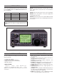
INTRODUCTION DANGER This service manual describes the latest service information for the IC-910H VHF/UHF ALL MODE TRANSCEIVER at the time of publication. NEVER connect the transceiver to an AC outlet or to a DC power supply that uses more than 16 V. This will ruin the transceiver. DO NOT expose the transceiver to rain, snow or any liquids. VERSION No. VERSION SYMBOL #02 Europe EUR #04 Australia AUS #06 U.S.A.
TABLE OF CONTENTS SECTION 1 SPECIFICATIONS SECTION 2 INSIDE VIEWS 2-1 IC-910H . . . . . . . . . . . . . . . . . . . . . . . . . . . . . . . . . . . . . . . . . . . . . . . . . . . . . . . . . . . . . . . . . . . . . . . 2 - 1 2-2 UX-910 (OPTIONAL UNIT) . . . . . . . . . . . . . . . . . . . . . . . . . . . . . . . . . . . . . . . . . . . . . . . . . . . . . . . . .
SECTION 1 SPECIFICATIONS ■ GENERAL • Frequency coverage : (Unit: MHz) Version 144 MHz 430 (440) MHz 1200 MHz*1 U.S.A. Tx: 144.0–148.0 Rx: 136.0–174.0*2 Tx: 430.0–450.0 Rx: 420.0–480.0*3 Tx: 1240.0–1300.0 Rx: 1240.0–1320.0*4 Europe 144.0–146.0 430.0–440.0 1240.0–1300.0 Australia 144.0–148.0 430.0–450.0 1240.0–1300.0 Korea 144.0–146.0 430.0–440.0 1260.0–1300.0 *1 Optional UX-910 is installed. *2 Guaranteed range is 144.0–148.0 MHz. *3 Guaranteed range is 430.0–450.0 MHz.
■ RECEIVER • Receive system : VHF SSB, CW FM SSB, CW FM UHF • Intermediate frequencies Single conversion superheterodyne Double conversion superheterodyne Double conversion superheterodyne Triple conversion superheterodyne : (Unit: MHz) MAIN BAND 144 MHz 430 (440) MHz 1200 MHz • Sensitivity • Squelch sensitivity (threshold) • Selectivity SUB BAND 1st 2nd 3rd SSB 10.8500 — — CW 10.8491 — — 1st 2nd 3rd 10.9500 — — 10.9491 — — FM 10.8500 0.455 — 10.9500 0.455 — SSB 71.
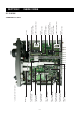
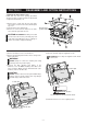
2-1 FM IF IC (IC401: TA31136FN) Analog master IC* (IC1701: µPC5023-077) AF power amplifier (IC1852: LA4445) D/A converter (IC1521: M62352GP) FM IF IC (IC951: TA31136FN) Crystal band pass filter (FI751: FL-129) TX IF amplifier* (Q1: 3SK131) Crystal band pass filter (FI151: FL-128) MAIN unit * Located under side of the point DDS IC (IC701: SC-1287) 144 MHz band VCO circuit DDS gate array (IC131: SC-1246A) Reference oscillator (X512: CR-452 30.
2-2 DRV board Varistor-A board TX balanced mixer Q501, Q502: 2SK302 D502: 1SV286 145 MHz power amplifier (Q651, Q652: 2SC5152) RX balanced mixer (Q511, Q512: 2SK1740) Pre-amplifier (Q507: 3SK177) TX/RX switching relay (RL700: AE5349) * Located under side of the point Drive amplifier (Q131: SRFJ7044) TX double balanced mixer D190: HSB88WS L190, L191: 617DB-1010 TX balanced mixer* (Q1, Q2: 2SK302) 440 MHz power amplifier (Q151, Q152: 2SC3102) Varistor-B board Varistor-C board RX balanced mixer
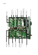
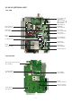
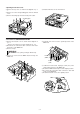
2-2 UX-910 (OPTIONAL UNIT) • TOP VIEW Power supply circuit for AG-1200 Q72: DTC144EU Q73, Q74: 2SC2712 RF pre-amplifier (Q281: NE34018) Power module IC (IC21: M57762-02) RF amplifier (Q271: 2SC5454) YGR amplifier (IC141: µPC1878G) TX 1st mixer (IC131: µPC8163TB) RX 1st mixer (IC241: µPC2721) PLL IC (IC501: TB31242) TX 1st IF amplifier (IC111: µPC2709) 1st LO VCO circuit RX 2nd mixer (Q221: 3SK166) DDS IC (IC661: SC-1246A) TX 2nd mixer (D82: HSB88WS) 2nd LO VCO circuit • BOTTOM VIEW Power supply c
SECTION 3 DISASSEMBLY AND OPTION INSTRUCTIONS • Opening the transceiver’s case Follow the case and cover opening procedures shown here when you want to install an optional unit or adjust the internal units, etc. q Remove the 5 screws from the top of the transceiver and 4 screws from the sides, then lift up the top cover. w Turn the transceiver upside down. e Remove 5 screws from the bottom of the transceiver, then lift up the bottom cover. Disconnect the speaker cable.
• Opening the PA unit cover r Slide the PA unit cover as shown below. q Remove the top cover as shown in the diagram on p. 31. w Remove 8 screws and grounding plate from the PA unit cover. e Remove fastening tape from the inside power cable. grounding plate • FL-132/FL-133 CW NARROW FILTER t Install FL-132 or FL-133 to the specified position on the MAIN unit. q Remove the bottom cover as shown in the diagram on p. 3-1. • Remove the UX-910 if you have installed it. (p.
• UT-102 VOICE SYNTHESIZER UNIT q Remove the bottom cover as shown in the diagram on p. 3-1. • Remove the UX-910 if you have installed it. (p. 3-1) w Remove the protective paper attached to the bottom of the UT-102 to expose the adhesive strip. e Plug UT-102 into J1801 on the MAIN unit as shown in the diagram at right. r Return the bottom cover to its original position.
y Install the CR-293 and solder the leads. u Return the PLL unit, PLL shield cover and bottom cover to their original positions. • CR-293 HIGH STABILITY CRYSTAL UNIT q Remove the bottom cover as shown in the diagram on p. 3-1. • Remove the UX-910 if you have installed it. (p. 3-1) w Remove 6 screws from the PLL shield cover, then lift up the PLL shield cover.
SECTION 4 CIRCUIT DESCRIPTION The filtered signals from the bandpass filter are mixed with 1st LO signals at the mixer circuit (Q511, Q512) to produce a 1st IF signal (10.85 MHz [Main] or 10.95 MHz [Sub]). The 1st LO signals (125.15 MHz–163.15 MHz) are PLL output frequency, which comes from the VHF VCO circuit (PLL unit; Q191, D191–D194).
4-1-6 10 MHz IF CIRCUIT (MAIN UNIT) 4-1-9 SQUELCH CIRCUIT (MAIN UNIT) The 10 MHz IF signal from the mixer circuit is passed through a monolithic filter (Fl51 [Main], Fl651 [Sub]) to suppress out-of-band signals. The filtered signal is amplified at the IF amplifier (Q51 [Main], Q651 [Sub]). The IF amplifier provides 20 dB gain. (1) FM mode A squelch circuit cuts out AF signals when no RF signal is received or the S-meter signal is lower than the [SQL] control setting level.
4-1-11 NOISE BLANKER CIRCUIT (MAIN UNIT) 4-1-13 S-METER CIRCUIT (MAIN UNIT) The noise blanker circuit detects pulse-type noises, and stops IF amplifier operation during detection. The S-meter circuit indicates the relative received signal strength while receiving and changes depending on the received signal strength. A portion of the 10 MHz IF signal from the bandpass filter (FI51 [Main], FI651 [Sub]) is amplified at the noise amplifier circuit (Q102, IC101, Q101 [Main], Q702, IC701, Q701 [Sub]).
While in SSB mode, the amplified signals from the buffer amplifier (Q1651) are then applied to the balanced modulator (IC201). 4-2-4 TRANSMIT IF AMPLIFIER CIRCUIT (MAIN UNIT) The modulated IF signal from a modulation circuit is applied to the IF amplifier circuit (Q1). The amplified IF signal is then applied to the VHF/UHF transmit circuit (PA unit) via the VHF /UHF switching circuit (D52, D53).
low-pass filter and UHF signal are high-pass filter, and then applied to the VHF and UHF power amplifier circuit separately. 4-3 PLL CIRCUITS IC-910H contains 2 PLL circuits and 1 local oscillator. The VHF and UHF PLL circuits adopt “Icom’s original I-loop PLL” to obtain very fast lock up times. 4-2-7 POWER AMPLIFIER CIRCUIT (PA UNIT) The power amplifier circuit amplifies the RF signals to the specified output power.
The passed signals are then applied to the RF amplifier circuit. The amplified signals are passed through the bandpass filter (FI1) to suppress spurious components, and are amplified at the pre-drive amplifier (Q36, Q38) and power module (IC21) to obtain a stable 10 W of output power.
SECTION 5 ADJUSTMENT PROCEDURES 4-1 PREPARATION BEFORE SARVICING ■ REQUIRED TEST EQUIPMENT EQUIPMENT GREDE AND RANGE EQUIPMENT DC power supply Output voltage Current capacity : 13.8 V DC : 30 A or more RF power meter (terminated type) Measuring range Frequency range Impedance SWR : : : : Frequency counter Frequency range Frequency accuracy Sensitivity : 0.1–100 MHz : ±0.
5-2 PLL ADJUSTMENTS ADJUSTMENT ADJUSTMENT CONDITION MEASUREMENT VALUE ADJUSTMENT POINT UNIT LOCATION UNIT ADJUST 1 • Display frequency: Any • Receiving PLL Connect an RF voltmeter or spectram analyzer to check point J541. –10 dBm (or more than –11.5 dBm, when R570 is in maximum position.) PLL R570 REFERENCE 1 • Display frequency: Any • Receiving FREQUENCY PLL Connect an RF voltmeter or spectram analyzer to check point P551.
• PLL AND MAIN UNITS R570 30.2 MHz level adjustment L193 144M lock voltage adjustment P701 P251 Sub BFO level check point 144M LO level check point X512 CP100 Reference frequency adjustment 144M lock voltage check point J541 P551 30.
5-4 RECEIVER ADJUSTMENTS Receiver adjustments must be performed after software adjustment (0) and (1). SUB band must be OFF when adjusting MAIN band, or main AF volume (max.counter clockwise) and SQL volume (max. clockwise) must be set when adjusting SUB band. ADJUSTMENT 144 M RECEIVER PEAK/GAIN MEASUREMENT ADJUSTMENT CONDITION 1 • Display frequency: Any • Disconnect P501 (PA unit) from J51 on the MAIN unit. • Connect a standard signal generator to [VHF ANT] connector and set as: Frequency : 146.
• PA UNIT 144M receiver peak/gain adjustment R547 L521 P501 144M receiver peak/gain check point • MAIN UNIT R857 144M peak adjustment for main band 144M total gain adjustment for sub band L353 L853 L354 L852 R360 144M total gain adjustment for main band L851 144M peak L653 L352 144M peak adjustment for main band adjustment for sub band L652 L53 L52 L651 L51 J51 144M receiver peak/gain pre-setting 5-5
RECEIVER ADJUSTMENTS (continued) ADJUSTMENT ADJUSTMENT CONDITION MEASUREMENT VALUE ADJUSTMENT POINT UNIT LOCATION UNIT ADJUST 430 M PEAK 1 • Display frequency: 435.0200 MHz • Mode : FM (MAIN BAND) • Connect a standard signal generator to [UHF ANT] connector and set as: Frequency : 435.0200 MHz Level : 1 µV* (–107 dBm) Modulation : 1 kHz/±5.0 kHz Dev. • Receiving MAIN Connect a digital multimeter or oscilloscope to check point CP851.
• PA UNIT L283 430M peak adjustment for main band L281 430M peak L282 adjustment L280 for sub band L23 L22 R61 430M total gain adjustment for main band • MAIN UNIT CP851 430M peak check point for main band CP852 430M peak check point for sub band CP101 Noise blanker check point for main band L703 Noise blanker adjustment Noise blanker adjustment for main band L704 for sub band L102 L103 CP701 Noise blanker check point for sub band 5-7
5-5 TRANSMITTER ADJUSTMENTS ADJUSTMENT MEASUREMENT ADJUSTMENT CONDITION UNIT VALUE LOCATION ADJUSTMENT POINT UNIT ADJUST PA R131 1 • Preset R131, R135, R150, R650 (PA unit) to max. counter clockwise. PA UNIT • Preset R3, R138, R503 (PA unit) to center position. PRESETTING • Preset C154, C659 (PA unit) to center position as illustration at right. IDLING CURRENT (for 144 M) 1 • Display frequency: [EUR], [KOR] 145.0000 MHz [USA-1], [AUS] 146.
• PA UNIT P501 RF peak pre-setting for 144 M C154 R503 L1 PA unit pre-setting C659 L2 RF peak adjustment for 430M Idling current adjustment for 144M RF peak adjustment for 430M R3 R138 PA unit pre-setting R131 P1 R135 RF peak pre-setting for 430M R650 R150 Idling current adjustment for 430M • MAIN UNIT R206 Carrier suppression R215 adjustment L2 L3 5-9 IF peak adjustment
TRANSMITTER ADJUSTMENTS (continued) ADJUSTMENT IF TOTAL GAIN ADJUSTMENT CONDITION 1 • Display frequency: Any • Mode : USB • MIC gain : Center • Disconnect P501 (PA unit) from J51 on the MAIN unit. • Connect an audio generator to [MIC] connector and set as: Frequency : 1.5 kHz Level : 2 mVrms • Transmitting MEASUREMENT UNIT LOCATION MAIN Connect an RF voltmeter to check point J51 via the JIG cable (B).
• MAIN UNIT R202 Drive level adjustment CP1613 IC APC pre-setting R1613 IC APC adjustment R3 IF total gain adjustment J51 IF total gain /Drive level check point • PA UNIT P501 IF total gain /Drive level pre-setting R503 Total gain adjustment for 144M R3 Total gain adjustment for 430M R504 LO leak adjustment for 144M 5 - 11
5-6 SOFTWARE ADJUSTMENT ADJUSTMENT ADJUSTMENT CONDITION DISPLAY ENTERING 1 • Enter software adjustment mode: SOFTWARE 1 Turn power OFF. ADJUSTMENT 2 Terminate the [REMOTE] jack with a 3.5(d) mm mini-plug. 3 While pushing [RIT] and [SATELLITE] keys, turn power ON. OPERATION The display shows the selection item scleen for the adjustment mode, push [0]–[9] key to select adjustment item. Once enterring adjustment mode, use [UP]/[DOWN] key to skip/back items, or [ENT] to return the selection item screen.
SOFTWARE ADJUSTMENT (continued) ADJUSTMENT ADJUSTMENT CONDITION DISPLAY ADJUSTMENT 1 • Enter software adjustment mode (Refer page 5-12). ITEM (2) • Push [2] key to enter the S-meter adjustS-METER ment (MAIN BAND) • Connect an SSG to [VHF ANT] connector and set as : Frequency : 146.0200 MHz Level : OFF • Receiving (SUB BAND) OPERATION Push [RIT] key to store the “S0” level into memory, and to step next. USB 2 • Set an SSG as Frequency Level • Receiving : : 146.0200 MHz : 3.
SOFTWARE ADJUSTMENT (continued) ADJUSTMENT S-METER (SUB BAND) ADJUSTMENT CONDITION 10 • Set an SSG as Frequency Level • Receiving : : 146.0200 MHz : OFF 11 • Set an SSG as Frequency Level Modulation • Receiving : : 146.0200 MHz : 3.2 µV* (–97 dBm) : OFF 12 • Set an SSG as Frequency Level • Receiving : : 146.0200 MHz : 32 µV* (–77 dBm) ADJUSTMENT 1 • Connect an SSG and set as ITEM (3) Frequency NOISE SQL Level (MAIN BAND) Modulation • Receiving (SUB BAND) to [VHF ANT] connector : : 146.
SOFTWARE ADJUSTMENT (continued) ADJUSTMENT ADJUSTMENT CONDITION ADJUSTMENT 1 • Connect an SSG and set as ITEM (4) Frequency CENTER Level (MAIN BAND) Modulation • Receiving to [VHF ANT] connector : : 146.0200 MHz : 5.6 µV* (–92 dBm) : OFF 2 DISPLAY FM Push [RIT] key to store the AFC center for FM mode into memory, and to step next. FMN Push [RIT] key to store the AFC center for FM narrow mode into memory, and to step next.
SOFTWARE ADJUSTMENT (continued) ADJUSTMENT ADJUSTMENT CONDITION DISPLAY ADJUSTMENT 1 • Enter software adjustment mode (Refer page 5-12). ITEM (6) • Push [6] key to enter the RF peak adjustRF PEAK ment for TX. • Connect an RF power meter to [VHF ANT] connector. 2 • Connect an SSG to P501 on the PA unit via the JIG cable (A) and set as: Frequency : 10.850 MHz Level : 18 mV* (–22 dBm) Modulation : OFF Push [RIT] key to strat transmitting. USB USB • Pushing [SET] key, tune the [MAIN DIAL] to maximum.
SOFTWARE ADJUSTMENT (continued) ADJUSTMENT TX POWER/ METER (for 430 M) ADJUSTMENT CONDITION DISPLAY 7 • Connect an RF power meter to [UHF ANT] connector. CW OPERATION Push [RIT] key to strat transmitting. 8 CW Tune the [MAIN DIAL] to 75 W (High power). Push [RIT] key to store the adjustment value into memory, and to step next. 9 CW Tune the [MAIN DIAL] to 37.5 W (Middle power). Push [RIT] key to store the adjustment value into memory, and to step next.
5-7 UX-910 ADJUSTMENTS ADJUSTMENT ADJUSTMENT CONDITION MEASUREMENT UNIT VALUE LOCATION ADJUSTMENT POINT UNIT ADJUST 2ND LO LOCK 1 • Connect an optional UX-910 (1200 MAIN Connect a digital (UX-910) multimeter or oscilloMHz band unit). VOLTAGE scope to check point • Display frequency: 1270.5000 MHz CP701. • Receiving 2.6–3.8 V Verify 1ST LO LOCK 1 • Display frequency: 1240.0000 MHz MAIN Connect a digital (UX-910) multimeter or oscillo• Receiving VOLTAGE scope to check point CP501. 6.0–7.
R67 APC adjustment CP321 Idling check point CP401 APC check point CP322 CP15 Idling check point APC check point R288 Attenuator adjustment C332 R37 Power ballance adjustment APC adjustment R13 R61 Idling adjustment APC adjustment CP501 1st LO lock voltage check point R83 Transmitter gain adjustment R224 Receiver gain adjustment CP701 2nd LO lock voltage check point CP311 Receiver gain check point 5 - 19
UX-910 ADJUSTMENTS (continued) ADJUSTMENT APC ADJUSTMENT CONDITION 1 • Display frequency: 1270.0000 MHz • Mode : CW • Connect an SSG to the check point CP311 and set as : Frequency : 10.8500 MHz • Transmitting 2 • Transmitting 3 • Transmitting MEASUREMENT VALUE UNIT LOCATION Rear panel Connect an RF power meter to [12 ANT]. 13 W MAIN Connect a digital (UX-910) multimeter or oscilloscope to check point CP15. 3.0 V Rear panel Connect an RF power meter to [12 ANT].
R67 APC adjustment CP401 APC check point CP15 APC check point R37 APC adjustment R61 APC adjustment CP311 Pre-setting for APC adjustment 5 - 21
SECTION 6 PARTS LIST 6-1 IC-910 [DISPLAY BOARD] [FRONT UNIT] REF NO. ORDER NO. REF NO. DESCRIPTION W1 W2 W3 W4 W5 W6 8900006700 8900006700 8900006700 8900009240 8900006700 8900006700 CABLE CABLE CABLE CABLE CABLE CABLE EP1 EP2 6910012480 E.OTHER 6450001230 E.OTHER OPC-645 OPC-645 OPC-645 OPC-909 OPC-645 OPC-645 (N:6 L:60) (N:6 L:60) (N:6 L:60) (P=1 N=10 L=110) (N:6 L:60) (N:6 L:60) RMS20-250-201-1R HLJ0999-01-480 [DISPLAY BOARD] REF NO. ORDER NO.
[DISPLAY BOARD] REF NO. R57 R58 R59 R60 R61 R66 R67 R68 R69 R70 R71 R72 R73 R74 R75 R76 R77 R78 R79 R80 R81 R82 R83 R87 R88 R90 R91 R92 R93 R94 R95 R96 R97 R98 R100 R101 R102 R103 R104 R105 R106 R107 R108 R109 R110 R111 R112 R113 R114 R115 R116 R117 R118 R123 R124 R125 R126 R127 R128 R129 R130 R131 R132 R133 R134 R135 R136 R137 R138 R139 R140 R141 R150 R151 R152 R153 R154 R155 R156 R157 R158 R159 ORDER NO.
[DISPLAY BOARD] REF NO. ORDER NO. [DISPLAY BOARD] REF NO.
[RIT BOARD] REF NO. ORDER NO. [PLL UNIT] DESCRIPTION R2 7210003090 VARIABLE RV-316 (RK0972210C05 10KB/10KB) J1 6510022570 S.CONNECTOR 06FMN-BMTTR-A-TBT EP1 0910052661 PCB B 5461A [JACK BOARD] REF NO. ORDER NO. DESCRIPTION L1 6200003950 S.COIL HF50ACC 322513-T R1 R2 7030006070 S.RESISTOR 7030006070 S.RESISTOR ERJ12YJ101U (100 Ω) ERJ12YJ101U (100 Ω) C1 C2 C3 4030006860 S.CERAMIC 4030006860 S.CERAMIC 4030006860 S.
[PLL UNIT] REF NO. [PLL UNIT] ORDER NO. REF NO. DESCRIPTION L424 L425 L471 L473 L474 L511 L541 L551 L552 L553 L599 L601 L602 L604 L700 L701 L702 L704 6200005720 6200005700 6200005010 6200005720 6200001830 6200001830 6200004950 6150005090 6150005090 6200002180 6200005010 6200003660 6200002610 6200002000 6200005010 6200003660 6200002610 6200002000 S.COIL S.COIL S.COIL S.COIL S.COIL S.COIL S.COIL S.COIL S.COIL S.COIL S.COIL S.COIL S.COIL S.COIL S.COIL S.COIL S.COIL S.
[PLL UNIT] REF NO. R427 R474 R475 R476 R477 R478 R479 R481 R482 R483 R501 R502 R503 R515 R538 R541 R542 R543 R544 R545 R547 R548 R551 R552 R553 R554 R555 R556 R557 R558 R559 R568 R569 R570 R571 R572 R601 R602 R603 R604 R605 R606 R607 R608 R609 R610 R611 R612 R613 R614 R615 R616 R617 R618 R619 R620 R621 R622 R623 R625 R626 R627 R628 R629 R630 R631 R701 R702 R703 R704 R705 R706 R707 R708 R709 R710 R711 R712 R713 R714 R715 R716 [PLL UNIT] ORDER NO.
[PLL UNIT] REF NO. C192 C193 C194 C196 C198 C213 C214 C215 C216 C217 C229 C251 C253 C254 C261 C262 C263 C273 C274 C275 C276 C277 C278 C279 C280 C281 C283 C284 C301 C302 C303 C304 C306 C308 C310 C312 C314 C321 C322 C323 C325 C327 C329 C330 C331 C332 C333 C334 C335 C336 C337 C339 C340 C341 C342 C343 C344 C345 C347 C348 C350 C362 C363 C364 C365 C366 C368 C369 C370 C371 C372 C373 C374 C375 C376 C377 C381 C382 C383 C391 C392 C393 ORDER NO.
[PLL UNIT] REF NO. [MAIN UNIT] ORDER NO. DESCRIPTION C705 C708 C709 C710 C711 C713 C714 C715 C716 C717 C718 C719 C720 C721 4030007160 4030007110 4030006900 4030006900 4030006900 4030006880 4030006900 4030006900 4030006900 4030006900 4030011600 4550006700 4030007130 4030007130 S.CERAMIC S.CERAMIC S.CERAMIC S.CERAMIC S.CERAMIC S.CERAMIC S.CERAMIC S.CERAMIC S.CERAMIC S.CERAMIC S.CERAMIC S.TANTALUM S.CERAMIC S.CERAMIC J1 J541 6510022540 S.
[MAIN UNIT] [MAIN UNIT] REF NO. ORDER NO.
[MAIN UNIT] [MAIN UNIT] REF NO. ORDER NO.
[MAIN UNIT] REF NO. R364 R365 R368 R369 R371 R372 R374 R375 R401 R402 R403 R404 R405 R406 R407 R408 R409 R410 R411 R412 R413 R414 R417 R418 R419 R420 R421 R456 R457 R458 R459 R462 R463 R464 R465 R466 R467 R468 R469 R470 R471 R472 R473 R474 R475 R476 R477 R478 R479 R481 R482 R484 R485 R486 R487 R488 R489 R490 R491 R492 R495 R496 R497 R498 R499 R651 R652 R653 R654 R655 R657 R658 R659 R660 R661 R662 R663 R664 R665 R666 R667 R702 [MAIN UNIT] ORDER NO.
[MAIN UNIT] REF NO. ORDER NO.
[MAIN UNIT] REF NO. ORDER NO.
[MAIN UNIT] REF NO. C59 C60 C61 C62 C101 C102 C103 C104 C106 C107 C108 C110 C113 C115 C116 C117 C118 C119 C121 C151 C152 C153 C156 C157 C158 C159 C160 C161 C162 C201 C202 C203 C204 C205 C206 C207 C208 C209 C210 C211 C212 C213 C214 C215 C216 C217 C218 C219 C251 C252 C253 C254 C255 C257 C258 C259 C260 C261 C262 C266 C304 C305 C306 C307 C308 C309 C310 C311 C312 C313 C314 C340 C342 C344 C345 C352 C353 C354 C355 C356 C357 C358 ORDER NO.
[MAIN UNIT] REF NO. ORDER NO.
[MAIN UNIT] REF NO. ORDER NO.
[PA UNIT] [PA UNIT] REF NO. ORDER NO. IC40 IC200 IC240 IC501 IC502 IC701 1110004080 1110003320 1110003320 1110004080 1110003320 1180001110 S.IC S.IC S.IC S.IC S.IC S.
[PA UNIT] REF NO. L71 L72 L97 L102 L103 L117 L118 L122 L123 L130 L131 L132 L133 L134 L151 L152 L153 L154 L180 L181 L182 L183 L184 L185 L186 L190 L191 L192 L194 L195 L196 L201 L202 L203 L205 L207 L220 L221 L222 L223 L224 L225 L240 L241 L242 L243 L244 L245 L246 L247 L260 L261 L262 L263 L264 L267 L268 L269 L280 L281 L282 L283 L301 L305 L306 L321 L381 L382 L391 L501 L502 L503 L504 L506 L507 L510 L512 L513 L514 L515 L516 L517 [PA UNIT] ORDER NO.
[PA UNIT] REF NO. R108 R110 R111 R117 R118 R121 R122 R123 R124 R125 R126 R127 R130 R131 R132 R133 R134 R135 R136 R137 R138 R150 R151 R152 R153 R154 R170 R171 R180 R182 R183 R184 R185 R186 R187 R188 R189 R190 R191 R196 R199 R200 R201 R203 R204 R205 R206 R208 R211 R212 R213 R214 R215 R220 R221 R222 R223 R224 R225 R226 R227 R228 R230 R240 R242 R244 R245 R246 R247 R248 R249 R250 R251 R260 R261 R262 R263 R264 R265 R266 R267 R268 [PA UNIT] ORDER NO.
[PA UNIT] REF NO. [PA UNIT] ORDER NO. REF NO.
[PA UNIT] REF NO. C139 C140 C141 C142 C143 C144 C145 C146 C147 C148 C149 C150 C151 C152 C153 C154 C155 C156 C157 C158 C159 C160 C161 C162 C163 C164 C165 C166 C167 C168 C169 C171 C172 C173 C174 C175 C176 C177 C178 C179 C180 C181 C182 C183 C184 C185 C186 C187 C188 C189 C190 C191 C192 C193 C194 C195 C196 C197 C198 C199 C200 C201 C202 C203 C204 C205 C206 C207 C208 C209 C210 C212 C213 C214 C215 C216 C217 C218 C219 C220 C221 C222 ORDER NO.
[PA UNIT] REF NO. C307 C308 C309 C310 C311 C312 C313 C314 C318 C319 C320 C321 C322 C323 C324 C325 C326 C327 C328 C329 C330 C331 C332 C333 C335 C338 C339 C340 C341 C343 C345 C346 C347 C348 C350 C351 C354 C356 C357 C361 C364 C367 C368 C369 C370 C371 C372 C373 C374 C375 C379 C381 C382 C383 C384 C391 C392 C393 C394 C397 C398 C399 C401 C402 C403 C404 C405 C406 C407 C408 C411 C412 C413 C414 C415 C416 C417 C418 C419 C501 C502 C503 [PA UNIT] ORDER NO.
[PA UNIT] REF NO. C607 C608 C609 C610 C611 C612 C613 C614 C616 C618 C619 C620 C621 C631 C632 C641 C642 C643 C644 C645 C646 C647 C648 C649 C650 C651 C652 C653 C654 C655 C656 C657 C658 C659 C661 C663 C664 C665 C667 C668 C669 C670 C671 C672 C673 C674 C675 C676 C677 C678 C679 C680 C681 C682 C683 C684 C685 C686 C687 C688 C689 C690 C691 C692 C693 C694 C696 C697 C701 C702 C703 C704 C705 C706 C707 C708 C710 C711 C712 C713 C714 C715 ORDER NO.
[PA UNIT] REF NO. F300 F301 F302 [DRV BOARD] ORDER NO. REF NO.
6-2 UX-910 [MAIN UNIT] — UX-910 [MAIN UNIT] REF NO. ORDER NO. IC21 IC31 IC111 IC131 IC141 IC161 IC162 IC181 IC201 IC241 IC301 IC311 IC501 IC502 IC601 IC610 IC621 IC661 IC701 IC761 IC762 1150002020 1110001220 1110004080 1110005150 1110001890 1180002040 1180001070 1110004080 1110004080 1110004470 1130007570 1130006800 1130009370 1130009580 1130004830 1130007260 1130004830 1140007880 1110001900 1110004460 1130003830 IC S.IC S.IC S.IC S.IC REG S.IC S.IC S.IC S.IC S.IC S.IC S.IC S.IC S.IC S.IC S.IC S.IC S.
[MAIN UNIT] — UX-910 REF NO. ORDER NO. [MAIN UNIT] — UX-910 REF NO.
[MAIN UNIT] — UX-910 REF NO. R288 R301 R311 R312 R342 R501 R502 R503 R504 R505 R506 R511 R512 R514 R515 R516 R517 R518 R519 R531 R533 R541 R542 R543 R544 R547 R551 R553 R554 R555 R556 R557 R603 R604 R605 R606 R607 R610 R611 R612 R613 R621 R622 R623 R624 R625 R626 R627 R628 R629 R630 R631 R633 R634 R635 R636 R637 R638 R639 R640 R641 R642 R643 R644 R645 R648 R651 R652 R661 R662 R663 R664 R681 R682 R683 R684 R701 R702 R719 R722 R723 R724 ORDER NO.
[MAIN UNIT] — UX-910 REF NO. C65 C66 C67 C69 C70 C71 C72 C73 C74 C76 C77 C79 C80 C81 C82 C83 C84 C85 C86 C87 C88 C89 C90 C91 C92 C93 C94 C95 C96 C97 C98 C99 C100 C101 C102 C103 C104 C105 C106 C111 C112 C114 C121 C122 C123 C124 C125 C130 C131 C132 C133 C134 C135 C136 C137 C138 C140 C141 C142 C143 C144 C145 C146 C147 C148 C149 C150 C151 C155 C160 C161 C162 C163 C164 C165 C166 C167 C168 C169 C170 C171 C172 ORDER NO.
[MAIN UNIT] — UX-910 REF NO. C287 C288 C289 C290 C292 C293 C294 C295 C297 C298 C299 C300 C301 C302 C304 C305 C306 C310 C311 C312 C313 C314 C315 C316 C317 C318 C320 C321 C322 C323 C324 C325 C326 C327 C328 C329 C330 C331 C332 C333 C334 C335 C336 C337 C501 C502 C503 C504 C505 C506 C507 C508 C509 C510 C511 C512 C513 C514 C515 C516 C517 C518 C520 C522 C523 C524 C531 C532 C533 C534 C535 C536 C537 C538 C541 C542 C543 C544 C545 C546 C548 C549 ORDER NO.
[MAIN UNIT] — UX-910 REF NO. ORDER NO. [MAIN UNIT] — UX-910 REF NO. ORDER NO.
SECTION 7 MECHANICAL PARTS [FRONT UNIT] REF. NO. EP1 EP2 MP1 MP2 MP4 MP5 MP6 MP7 MP9 MP13 MP14 MP15 MP17 MP19 MP20 MP22 MP23 MP25 MP31 MP32 MP33 MP34 MP35 MP36 MP38 [COVER PARTS] ORDER NO.
[PA UNIT] REF. NO. ORDER NO.
SECTION 8 SEMI-CONDUCTOR INFORMATION • TRANSISTORS AND FET’S 2SA1162 GR (Symbol: SG) 2SA1586 GR (Symbol: SG) 2SA1588 GR (Symbol: ZG) 2SB1132 T100 R (Symbol: BAR) 2SB1133 R (Symbol: B1133) E B B B B C C C C E E B E C E 2SB1201 S (Symbol: B1201) 2SC2712 BL (Symbol: BL) 2SC2712 GR (Symbol: LG) BC 2SC2714 O (Symbol: QO) E 2SC3102 (Symbol: None) E C B C C E E E B C C C C E E B B B E E B E B E 2SC3356 T2B (Symbol: R24) 2SC3357 T2 (Symbol: RK) 2SC4081 T107 R (Symbol: BR
2SK2855 (Symbol: UT) 2SK2973 (Symbol: K1) G G S S S D D 3SK241 R (Symbol: DU) CPH3404-TL (Symbol: KD) D 2SK2975 G2 3SK131 T2 LA (Symbol: V12) G S D DTA114 EE TL (Symbol: 14) G1 DTC114EUA T106 (Symbol: 24) NE34018 T1 (Symbol: V63) RN2425 (Symbol: RE) G S DTC144EUA T106 (Symbol: 26) G2 D B FMW1 T148 (Symbol: W1) B1 C C E SRFJ7044 (Symbol: SRFJ7044) B1 D S XP4312 (Symbol: 7T) C1 E1 G G D XP4315 (Symbol: CB) S E B2 S XP4601 (Symbol: 5C) E1 C1 E1 C1 B1 B2 B1 B2
• DIODES 1SS301 (Symbol: B3) 1SS355 (Symbol: A) 1SS375-TL (Symbol: FH) 1SS385 (Symbol: 09) A1 1SV214 (Symbol: T1) pink A1 C A C C A2 A C A2 1SV217 (Symbol: T6) 1SV237 (Symbol: BB) 1SV239 (Symbol: TC) 1SV265 TL (Symbol: LV) 1SV286 (Symbol: T7) NC A1 A C1 A C A2 1SV307 (Symbol: TX) C A C C2 1SV308 (Symbol: TX) DA221 (Symbol: K) DAN202 U T107 (Symbol: N) DAN222TL (Symbol: N) A1 A C A C C A C A2 DAP202K T146 (Symbol: P) DAP222 TL (Symbol: P) C1 HSM88AS TR (Symbol: C1)
BOARD LAYOUTS 9-1 VR-A BOARD 9-3 RIT BOARD • TOP VIEW • TOP VIEW 2 6 2 J1 1 5 1 5 to DISPLAY board J10 to DISPLAY board J2 9-2 VR-B BOARD • TOP VIEW 2 6 GND SAVR NC NC SSVR +5V J1 1 5 to DISPLAY board J11 6 GND RIVR NC GND MAVR NC NC MSVR +5V J1 NC SFVR +5V SECTION 9 9-1
• BOTTOM VIEW (RIT BOARD) • BOTTOM VIEW (VR-A BOARD) • BOTTOM VIEW (VR-B BOARD) 9-2
1-1-32, Kamiminami, Hirano-ku, Osaka 547-0003, Japan Phone : 06 6793 5302 Fax : 06 6793 0013 URL : http://www.icom.co.jp/world/index.html Icom America Inc. Icom (Europe) GmbH < Corporate Headquarters > Communication Equipment Himmelgeister Str. 100, D-40225 Düsseldorf, Germany Phone : 0211 346047 Fax : 0211 333639 URL : http://www.icomeurope.com 2380 116th Avenue N.E., Bellevue, WA 98004, U.S.A. Phone : (425) 454-8155 Fax : (425) 454-1509 URL : http://www.icomamerica.
1-1-32, Kamiminami, Hirano-ku Osaka 547-0003, Japan S-13714HZ-C1 © 2001 Icom Inc.