SERVICE MANUAL VHF TRANSCEIVER iF110S iF111S iF121S
INTRODUCTION DANGER This service manual describes the latest service information for the IC-F110S, IC-F111S and IC-F121S VHF MOBILE TRANSCEIVER at the time of publication. NEVER connect the transceiver to an AC outlet or to a DC power supply that uses more than 16 V. This will ruin the transceiver. DO NOT expose the transceiver to rain, snow or any liquids. MODEL VERSION SYMBOL Europe EUR General GEN IC-F111S General GEN IC-F121S U.S.A.
EXPLICIT DEFINITIONS FREQUENCY COVERAGE CHANNEL SPACING 12.5 kHz/ 25.0 kHz 136 – 174 MHz Narrow/Wide-type Narrow/Middle-type 15.0 kHz/ 30.0 kHz 15.0 kHz/ 20.0 kHz TABLE OF CONTENTS SECTION 1 SPECIFICATIONS SECTION 2 INSIDE VIEW SECTION 3 DISASSEMBLY INSTRUCTIONS SECTION 4 CIRCUIT DESCRIPTION 4-1 RECEIVER CIRCUITS . . . . . . . . . . . . . . . . . . . . . . . . . . . . . . . . . . . . . . . . . . . . . . . . . . . . . . . . . . . .4 - 1 4-2 TRANSMITTER CIRCUITS . . . . . . . . . . . . . . . .
SECTION 1 SPECIFICATIONS Measurement method [GEN], [USA] [EUR] EIA-152-C/204D or TIA-603 EN 300 086 Frequency coverage N/W: (12.5 kHz; Narrow/25 kHz; Wide): 8K50F3E/16K0F3E (12.5 kHz; Narrow/25 kHz; Wide): 11K0F3E/16K0F3E (15 kHz; Narrow/30 kHz; Wide): 11K0F3E/16K0F3E N/M: (12.5 kHz; Narrow/20 kHz; Middle): 8K50F3E/14K0F3E Type of emission GENERAL 136.000–174.000 MHz Free: 8 channels, Bank: 4 channels × 2 banks Number of conventional channels 50 Ω nominal (SO-293) Antenna impedance 13.
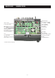
SECTION 2 INSIDE VIEW Final FET module IC3: RA30H1317 [25W] S-AV32 [50W] Antenna switch/ Low-pass filter circuit CPU 5V regulator* (IC10: AN78L05M) 8V regulator (IC9: TA7808F) Mixer* (Q3: 3SK299) 2nd IF filter* (FI2: ALFYM450F=K) VCO circuit D/A converter* (IC6: M62363FP-650C) AF amplifier (IC8: LA4425A) IF IC (IC1: TA31136FN) Reference crystal oscillator* (X2: CR-740 15.3 MHz) 1st IF filter (FI1: FL-335) PLL IC (IC4: MB15A02PFV-1) * Located under side of the point.
SECTION 3 DISASSEMBLY INSTRUCTIONS • Opening case and remove the front panel ➀ Unscrew 4 screws A, and remove the bottom cover. ➁ Disconnect the flat cable B from J2. ➂ Disconnect the cable C from J7. ➃ Unscrew 2 screws D , and remove the front unit in the ➅ Lift up the front portion of the main unit and remove it. direction of the arrow.
SECTION 4 CIRCUIT DESCRIPTION 4-1-3 1ST MIXER AND 1ST IF CIRCUITS (MAIN UNIT) 4-1 RECEIVER CIRCUITS 4-1-1 ANTENNA SWITCHING CIRCUIT (MAIN UNIT) The 1st mixer circuit converts the received signals to a fixed frequency of the 1st IF signal with the PLL output frequency. By changing the PLL frequency, only the desired frequency will pass through a MCF (Monolithic Crystal Filter; FI1) at the next stage of the 1st mixer.
4-1-5 AF AMPLIFIER CIRCUIT (MAIN UNIT) 4-2 TRANSMITTER CIRCUITS The AF amplifier circuit amplifies the demodulated AF signals to drive a speaker. 4-2-1 MICROPHONE AMPLIFIER CIRCUIT (MAIN AND FRONT UNITS) The microphone amplifier circuit amplifies audio signals within +6 dB/octave pre-emphasis characteristics from the microphone to a level needed for the modulation circuit. The AF signals from the FM IF IC (IC1, pin 9) are applied to the active filter circuit (IC16).
4-2-4 POWER AMPLIFIER CIRCUIT (MAIN UNIT) 4-3 PLL CIRCUITS The power amplifier circuit amplifies the driver signal to an output power level. 4-3-1 PLL CIRCUIT (MAIN UNIT) A PLL circuit provides stable oscillation of the transmit frequency and receive 1st LO frequency. The PLL output compares the phase of the divided VCO frequency to the reference frequency. The PLL output frequency is controlled by the divided ratio (N-data) of a programable divider.
4-4 POWER SUPPLY CIRCUITS 4-4-1 VOLTAGE LINES (MAIN UNIT) Line HV VCC 4-5-3 CPU (FRONT UNIT; IC1) Description The voltage from a DC power supply. The same voltage as the HV line which is controlled by the power switching circuit (Q23, Q24). When the [POWER] switch is pushed, the CPU outputs the “PWON” control signal to the power switching circuit to turn the circuit ON. Common 8 V converted from the VCC line by the 8V regulator circuit (IC9).
CPU-Continued Pin number Port name Description 41 PWON Outputs control signal for the power switching circuit (MAIN unit; Q24, Q23). 42 NWC Outputs IF bandwidth control signal. Low : While IF bandwidth is narrow. 43 AFON Outputs control signal for the AF mute circuit (MAIN unit; Q35, Q36, D29). High : While AF amplifier (MAIN unit; IC8) is activated. 44–46 OPT3– OPT1 I/O ports for the optional board control signals.
SECTION 5 ADJUSTMENT PROCEDURES 5-1 PREPARATION ■ ADJUSTMENT SOFTWARE INSTALLATION When you adjust the contents on pages 5-5 and 5-6, SOFTWARE ADJUSTMENT, the optional CS-F100S ADJ ADJUSTMENT SOFTWARE (Rev. 1.0 or later), *OPC-1122 JIG CABLE (modified OPC-1122 CLONING CABLE; see illustration below) are required. q Boot up Windows. - Quit all applications when Windows is running. w Insert the ‘CS-F100S’ into the appropriate CD drive. e Select ‘Run’ from the [Start] menu.
■ REQUIRED TEST EQUIPMENT EQUIPMENT GRADE AND RANGE EQUIPMENT DC power supply Output voltage Current capacity : 13.2 V DC : 15 A or more RF power meter (terminated type) Measuring range Frequency range Impedance SWR : : : : Frequency counter Frequency range : 0.
• Screen display exampe CS-F100S ADJ Rev.1.0 File Option COM 1: OPEN Connect 2 Reload (F5) Disp para 1 4 5 6 7 8 9 10 11 12 13 14 [A / D] VIN : 178 : B2h : 19.96 V TEMPS : 177 : B1h : 26.44 'C LVIN : 176 : B0h : 3.45 V SD : 23 : 17h : 0.45 V CH No.
5-2 PLL ADJUSTMENT MEASUREMENT ADJUSTMENT ADJUSTMENT CONDITIONS UNIT PLL LOCK VOLTAGE 1 • Operating freq. : 174.000 MHz • Receiving 2 • Output power • Transmitting ADJUSTMENT VALUE LOCATION MAIN Connect a digital multimeter or an oscilloscope to the check point, “LV”. : Low1 UNIT ADJUST 3.5 V MAIN C134 3.5 V C133 3 • Operating freq. : 136.000 MHz • Receiving 0.9–1.5 V Verify 4 • Output power • Transmitting 1.0–1.6 V : Low1 DC power supply 13.
5-3 SOFTWARE ADJUSTMENT Select an operation using [↑] / [↓] keys, then set specified value using [←] / [→] keys on the connected computer keyboard. ADJUSTMENT MEASUREMENT ADJUSTMENT CONDITION UNIT LOCATION VALUE REFERENCE FREQUENCY [TXF] 1 • Operating freq. : 174.000 MHz Rear Loosely couple a frequnecy • Output power : Low1 panel counter to the antenna connec• Connect the RF power meter or 50 Ω tor. dummy load to the antenna connector. • Transmitting OUTPUT POWER [Power (Hi)] 1 • Operating freq.
SOFTWARE ADJUSTMENT – continued Select an operation using [↑] / [↓] keys, then set specified value using [←] / [→] keys on the connected computer keyboard. ADJUSTMENT RX SENSITIVITY [BPF T1], [BPF T2] ADJUSTMENT CONDITION MEASUREMENT UNIT VALUE LOCATION MAIN Connect a SINAD meter with a Minimum distortion 1 • Operating freq. : 136.000 MHz level • IF bandwidth : Wide 4 Ω load to the external [SP] • Connect a standard signal generator to jack. the antenna connector and set as: Frequency : 136.
5-4 TRIMMER ADJUSTMENT • Make this adjustment if necessary (For example, when beep sound is too loud or too soft). • BE CAREFUL!: 5-tone calling beep sound becomes loud or soft when beep volume adjusts to loud or soft. MEASUREMENT ADJUSTMENT UNIT BEEP VOLUME ADJUSTMENT ADJUSTMENT CONDITIONS 1 • Operating freq. : Any • Receiving LOCATION FRONT Push any button except [POWER] FRONT switch, then verify the beep volume level.
SECTION 6 PARTS LIST [FRONT UNIT] REF NO. [FRONT UNIT] ORDER NO. REF NO. DESCRIPTION IC1 IC2 IC3 IC4 IC5 1140010890 1110005770 1130010390 1130009670 1110005340 S.IC S.IC S.IC S.IC S.IC Q1 Q2 Q3 1530002060 S.TRANSISTOR 1590001050 S.TRANSISTOR 1590000430 S.TRANSISTOR 2SC4081 T106 R DTC114TUA T106 DTC144EUA T106 D1 D2 D3 D4 D5 1790000950 1790000950 1790000950 1790000620 1790001250 MA8056-M (TX) MA8056-M (TX) MA8056-M (TX) MA77 (TX) MA2S111-(TX) X1 6050009520 S.XTAL CR-520 (19.
[FRONT UNIT] REF NO. [MAIN UNIT] ORDER NO. REF NO. DESCRIPTION J2 6510022470 S.
[MAIN UNIT] REF NO. R5 R6 R7 R8 R9 R10 R11 R13 R14 R15 R16 R17 R18 R19 R20 R21 R22 R23 R25 R26 R27 R28 R29 R31 R32 R33 R34 R35 R36 R37 R38 R39 R40 R42 R43 R44 R45 R46 R48 R49 R50 R51 R52 R53 R54 R55 R56 R57 R58 R59 R60 R61 R62 R63 R67 R68 R69 R70 R71 R73 R74 R75 R76 R77 R78 R79 R80 R82 R83 R84 R85 R86 R89 R90 R91 R92 [MAIN UNIT] ORDER NO.
[MAIN UNIT] REF NO. R215 R216 R217 R218 R219 R220 R221 R222 R223 R224 R225 R226 R227 R228 R229 R230 R231 R232 R234 R235 R236 R237 R238 R240 R241 R242 R243 R244 R245 R247 R248 R249 R250 R251 R252 R261 R262 R263 R264 R265 R266 R267 R268 R269 R270 R271 R285 R287 R290 R291 R292 R297 R298 R304 R305 R310 R311 R312 R313 R314 R315 R316 R317 R318 R319 R320 R321 R322 C1 C2 C3 C4 C5 C6 C7 [MAIN UNIT] ORDER NO. REF NO.
[MAIN UNIT] REF NO. C92 C93 C94 C95 C96 C97 C99 C100 C102 C103 C104 C105 C106 C107 C108 C109 C110 C111 C113 C114 C115 C116 C117 C118 C119 C120 C121 C122 C123 C124 C126 C127 C129 C131 C132 C133 C134 C135 C136 C138 C139 C140 C141 C142 C143 C144 C145 C146 C147 C148 C149 C151 C152 C153 C154 C155 C156 C157 C158 C160 C161 C162 C163 C164 C165 C166 C167 C168 C169 C170 C172 C173 C174 C175 C176 C177 C178 C179 C180 C181 C182 C183 [MAIN UNIT] ORDER NO.
[MAIN UNIT] REF NO. [MAIN UNIT] ORDER NO. REF NO.
SECTION 7 MECHANICAL PARTS [CHASSIS PARTS] REF. NO. ORDER NO. [ACCESSORIES] DESCRIPTION J1 6510004880 Connector MR-DS-E 01 MP1 8010019060 8010019130 8110007820 8810008660 8810008660 8810008660 8810008660 8810009990 8810009990 8930058990 2601 chassis 2601 long chassis 2601 cover Screw PH BT M3 × Screw PH BT M3 × Screw PH BT M3 × Screw PH BT M3 × Screw PH BT M3 × Screw PH BT M3 × Shield sponge (V) MP2 MP3 MP4 MP5 MP6 MP7 MP8 MP10 [25W] [50W] 8 8 8 8 8 8 REF. NO. QTY.
MP4 (C) MP8 (C) J1 (C) W2 (M) MP1 (C) MP3 (M) J4 (M) MP1 (M) MP9 (M) MAIN UNIT MP7 (M) MP6 (C) MP5 (C) MP4 (M) R14 (F) MP5 (M) W1 (F) MP10 (M) MP3 (C) MP6 (M) J1 (F) MP7 (F) MP10 (F) MP2 (C) MP8 (F) MP3 (C) MP1 (F) MP4 (F) FRONT UNIT MP2 (M) MP2 (F) MP5 (F) SP1 (F) MP7 (C) MP9 (F) Unit abbreviations (F): FRONT UNIT (M): MAIN UNIT (C): CHASSIS PARTS MP3 (F) 7-2
SECTION 8 SEMI-CONDUCTOR INFORMATION • TRANSISTORS AND FET’S 2SA1577 T106 Q (Symbol: HQ) • DIODES 2SC3356 T1B R25 (Symbol: R25) B 2SC4081 T106 R (Symbol: BR) B B C E E 2SC5107 O (Symbol: MFO) 2SC4215 O (Symbol: QO) 2SD1664 T100Q (Symbol: DAQ) 1SS375-TL (Symbol: FH) 1SV239 (Symbol: TC) DA221 TL (Symbol: K) DAN222TL (Symbol: N) A C C E E 2SJ144 GR (Symbol: VG) 2SJ377 (Symbol: 4L) HVC350B (Symbol: B0) A1 B B C C E 2SC4226 T1 R25 (Symbol: R25) 2SC4116 BL (Symbol: LL) C C A C A
SECTION 9 BOARD LAYOUTS 9-1 FRONT UNIT • TOP VIEW 2 8 8V AFO MICE GND CLO PTT MIC CLI J1 1 to Microphone 7 9-1 4 1 5 8
GND TONE TENC NOIS NWC TMUT UNLK PLST CDEC SDEC OV12 RSSI LVIN TEMP BATV RXC AFON 5V CPU5 AFO J2 DIM DAST RMUT MMUT OPT3 OPT2 OPT1 BUSY SCK SI SO CIRQ CCS MIC EPTT HORNO BEEP PWON 8V GND • BOTTOM VIEW (FRONT UNIT) 33 64 1 2 to MAIN unit J2 32 48 17 49 16 11 10 20 1 1 14 8 1 7 39 40 9-2
DIM DAST RMUT MMUT OPT3 OPT2 OPT1 BUSY SCK SI SO CIRQ CCS MIC EPTT HORNO BEEP PWON 8V GND J1 PTTI PTTO MCOT MCIN NC BUSY NC SIGO OPT1 OPT2 OPT3 GND OPV3 OPV2 OPV1 5 4 8 1 1 15 30 39 to Optional unit 9-3 16 J2 GND TONE TENC NOIS NWC TMUT UNLK PLST CDEC SDEC OV12 RSSI LVIN TEMP BATV RXC AFON 5V CPU5 AFO 8 9 1 SPSP+ • TOP VIEW GND 5V VCC NC AFONO BEEPO NC DET DISC NC CCS CIRQ SO SI SCK 9-2 MAIN UNIT ANT CHASSIS J1 to DC cable W2 40 to FRONT unit J2 9 8 16 1 2 1 J7 2 1 to speaker 16 1 J
• BOTTOM VIEW (MAIN UNIT) SP 24 13 1 12 14 8 1 7 9-4 1 14 7 8
SECTION 10 BLOCK DIAGRAM 8V REF Q19 2SC4215 15.3 MHz REF RIPPLE FIL BUFF IC4 MB15A02PFV-1 PLL IC LOOP FIL D18 1SV239 FM MOD Q34 2SC4116 X3 Q11 2SC5107 Q10 2SC5107 BUFF BUFF BPF D14, D15 MA77 IF IC IF AMP NWC W/N SW DRIVE ATT FI1 FL-335 XTAL BPF 182.35 MHz-220.
SECTION 11 VOLTAGE DIAGRAMS 11-1 FRONT UNIT R3 1k R7 680 CH1 CH2 CH3 CH4 LP0 LP1 CP1 64 63 62 61 60 59 58 57 56 55 54 53 52 51 50 49 SO SCK EXST IC2 S-80942CNMC-G9C 5 C30 0.027 4 5.0V 1 OUT 2 VDD 3 VSS CD NC TEMP BATV C35 0.
11-2 MAIN UNIT MAIN UNIT (1) C427 220p[EUR] C115 33p C113 0.75p R77 10k 4 C118 0.5p 3 2 C122 33p 5 1 C357 0.1 TX: 0.1V RX: 4.4V R291 100k C297 22p Q16 DTC144EU R313 1k L38 80n C111 47p R78 1k c TXC RXC R35 100 R38 100k R34 100k C60 0.01 R290 680 X1 CDBC450CX24 R36 3.9k R33 330 MAIN UNIT (2) C64 0.001 C365 1.5p R37 2.7k(N/W) 4.7k(N/M) d R292 1k C75 10 R43 470 C348 0.001 R42 47k C63 47p C58 0.001 Q4 2SC4215 C65 0.001 Q5 DTC144EU C66 0.001 C70 100p R46 2.
5V CPU5V 8V Q28 XP6501 O G 3 I IC10 AN78L05M Q24 DTC144EU C430 0.001[EUR] 4 2 IC15 TA75S01F R195 1k R238 100k POWER ON: 4.8V OFF: 0V C251 0.1 C253 0.022 C246 0.1 I C252 0.1 1 2 R230 68k 5 4 IC8 LA4425A 3 D C295 10 F C431 100p AFO R226 100k BUS LINE2 11 - 3 C408 0.001 5 R197 10k C254 0.001 VCC R199 10k 1 3 Q35 DTC363EK Q36 DTC144EU R198 10k T8V C426 100p[EUR] AF ON: 4.8V OFF: 0V BUS LINE1 AFON AFONO D30 DAN222 Q31 2SJ144 D26 MA2S111 R225 10k C288 0.1 R224 47 C289 0.
1-1-32, Kamiminami, Hirano-ku, Osaka 547-0003, Japan S-13906HZ-C1VS-e © 2003 Icom Inc.
SERVICE MANUAL UHF TRANSCEIVER iF210S iF211S iF221S
INTRODUCTION DANGER This service manual describes the latest service information for the IC-F210S, IC-F211S and IC-F221S UHF MOBILE TRANSCEIVER at the time of publication. NEVER connect the transceiver to an AC outlet or to a DC power supply that uses more than 16 V. This will ruin the transceiver. MODEL VERSION SYMBOL DO NOT expose the transceiver to rain, snow or any liquids. DO NOT reverse the polarities of the power supply when connecting the transceiver.
EXPLICIT DEFINITIONS FREQUENCY COVERAGE CHANNEL SPACING Low Band 400-430 MHz Narrow/Wide-type 12.5 kHz/ 25.0 kHz High Band 440-490 MHz Narrow/Middle-type 12.5 kHz/ 20.0 kHz TABLE OF CONTENTS SECTION 1 SPECIFICATIONS SECTION 2 INSIDE VIEW SECTION 3 DISASSEMBLY INSTRUCTIONS SECTION 4 CIRCUIT DESCRIPTION 4-1 RECEIVER CIRCUITS . . . . . . . . . . . . . . . . . . . . . . . . . . . . . . . . . . . . . . . . . . . . . . . . . . . . . . . . . . . .4 - 1 4-2 TRANSMITTER CIRCUITS . . . . . . . .
SECTION 1 SPECIFICATIONS Measurement method [GEN], [USA] [EUR] EIA-152-C/204D or TIA-603 EN 300 086 Frequency coverage N/W: (12.5 kHz; Narrow/25 kHz; Wide): 8K50F3E/16K0F3E (12.5 kHz; Narrow/25 kHz; Wide): 11K0F3E/16K0F3E N/M: (12.5 kHz; Narrow/20 kHz; Middle): 8K50F3E/14K0F3E Type of emission GENERAL 400.000–430.000 MHz 440.000–490.000 MHz Free: 8 channels, Bank: 4 channels × 2 banks Number of conventional channels Power supply voltage (negative ground) 13.
SECTION 2 INSIDE VIEW Final FET module IC3 : RA30H4452M-21 [25W-H] : RA30H4047M-21 [25W-L] : RA45H4452M-21 [45W-H] : RA45H4047M-21 [45W-L] CPU 5V regulator* (IC10: AN78L05M) Antenna switch/ Low-pass filter circuit 8V regulator (IC9: TA7808F) Mixer* (Q3: 3SK299) 2nd IF filter* (FI2: ALFYM450F=K) VCO circuit D/A converter* (IC6: M62363FP-650C) AF amplifier (IC8: LA4425A) IF IC (IC1: TA31136FN) Reference crystal oscillator* (X2: CR-741 15.
SECTION 3 DISASSEMBLY INSTRUCTIONS • Opening case and removing the front unit q Unscrew 4 screws A, and remove the bottom cover. w Disconnect the flat cable B from J2. e Disconnect the cable C from J7. r Unscrew 2 screws D , and remove the front unit in the e Unscrew 8 screws H. r Remove the filter case I. t Unscrew the screw J. y Unsolder 3 points K from the antenna connector. u Unsolder 4 points L from IC3. direction of the arrow.
SECTION 4 CIRCUIT DESCRIPTION 4-1-3 1ST MIXER AND 1ST IF CIRCUITS (MAIN UNIT) 4-1 RECEIVER CIRCUITS 4-1-1 ANTENNA SWITCHING CIRCUIT (MAIN UNIT) The 1st mixer circuit converts the received signals to a fixed frequency of the 1st IF signal with the PLL output frequency. By changing the PLL frequency, only the desired frequency will pass through a MCF (Monolithic Crystal Filter; FI1) at the next stage of the 1st mixer.
4-1-5 AF AMPLIFIER CIRCUIT (MAIN UNIT) 4-2 TRANSMITTER CIRCUITS The AF amplifier circuit amplifies the demodulated AF signals to drive a speaker. 4-2-1 MICROPHONE AMPLIFIER CIRCUIT (MAIN AND FRONT UNITS) The microphone amplifier circuit amplifies audio signals within +6 dB/octave pre-emphasis characteristics from the microphone to a level needed for the modulation circuit. The AF signals from the FM IF IC (IC1, pin 9) are applied to the active filter circuit (IC16).
4-2-4 POWER AMPLIFIER CIRCUIT (MAIN UNIT) 4-3 PLL CIRCUITS The power amplifier circuit amplifies the driver signal to an output power level. 4-3-1 PLL CIRCUIT (MAIN UNIT) A PLL circuit provides stable oscillation of the transmit frequency and receive 1st LO frequency. The PLL output compares the phase of the divided VCO frequency to the reference frequency. The PLL output frequency is controlled by the divided ratio (N-data) of a programable divider.
4-4 POWER SUPPLY CIRCUITS 4-5-3 CPU (FRONT UNIT; IC1) 4-4-1 VOLTAGE LINES (MAIN UNIT) Description Line HV VCC The voltage from a DC power supply. The same voltage as the HV line which is controlled by the power switching circuit (Q23, Q24). When the [POWER] switch is pushed, the CPU outputs the “PWON” control signal to the power switching circuit to turn the circuit ON. Common 5 V for the CPU converted from the HV line by the CPU5V regulator circuit (IC10).
CPU-Continued Pin number Port name Description 41 PWON Outputs control signal for the power switching circuit (MAIN unit; Q23, Q24). 42 NWC Outputs IF bandwidth control signal. Low : While IF bandwidth is narrow. 43 AFON Outputs control signal for the AF mute circuit (MAIN unit; Q35, Q36, D29). High : While AF amplifier (MAIN unit; IC8) is activated. 44–46 OPT3– OPT1 I/O ports for the optional board control signals.
SECTION 5 ADJUSTMENT PROCEDURES 5-1 PREPARATION ■ ADJUSTMENT SOFTWARE INSTALLATION When you adjust the contents on pages 5-5 and 5-6, SOFTWARE ADJUSTMENT, the optional CS-F100S ADJ ADJUSTMENT SOFTWARE (Rev. 1.0 or later), *OPC-1122 JIG CABLE (modified OPC-1122 CLONING CABLE; see illustration below) are required. q Boot up Windows. - Quit all applications when Windows is running. w Insert the ‘CS-F100S’ into the appropriate CD drive. e Select ‘Run’ from the [Start] menu.
■ REQUIRED TEST EQUIPMENT EQUIPMENT GRADE AND RANGE DC power supply Output voltage Current capacity : 13.2 V DC : 15 A or more RF power meter (terminated type) Measuring range Frequency range Impedance SWR : : : : Frequency counter Frequency range : 0.
• Screen display exampe CS-F100S ADJ Rev.1.0 File Option COM 1: OPEN Connect 2 Reload (F5) Disp para 1 4 5 6 7 8 9 10 11 12 13 14 [A / D] VIN : 178 : B2h : 19.96 V TEMPS : 177 : B1h : 26.44 'C LVIN : 176 : B0h : 3.45 V SD : 23 : 17h : 0.45 V CH No.
5-2 PLL ADJUSTMENT MEASUREMENT ADJUSTMENT ADJUSTMENT CONDITIONS UNIT PLL LOCK VOLTAGE 1 • Operating freq. : 400.000 MHz [L] 440.000 MHz [H] • Receiving 2 • Output power • Transmitting ADJUSTMENT VALUE LOCATION MAIN Connect a digital multimeter or an oscilloscope to the check point, “LV”. : Low1 3 • Operating freq. : 430.000 MHz [L] 490.000 MHz [H] • Receiving 4 • Output power : Low1 • Transmitting UNIT ADJUST 1.0 V MAIN C133 1.0 V C134 3.3–4.4 V [L] 3.3–4.5 V [H] Verify 3.3–4.4 V [L] 3.3–4.
5-3 SOFTWARE ADJUSTMENT Select an operation using [↑] / [↓] keys, then set specified value using [←] / [→] keys on the connected computer keyboard. ADJUSTMENT MEASUREMENT ADJUSTMENT CONDITION UNIT LOCATION VALUE REFERENCE FREQUENCY [TXF] 1 • Operating freq. : 490.000 MHz Rear Loosely couple a frequnecy 490.0000 MHz [H] 430.000 MHz panel counter to the antenna connec- 430.0000 MHz [L] • Output power : Low1 tor. • Connect the RF power meter or 50 Ω dummy load to the antenna connector.
SOFTWARE ADJUSTMENT – continued Select an operation using [↑] / [↓] keys, then set specified value using [←] / [→] keys on the connected computer keyboard. ADJUSTMENT RX SENSITIVITY [BPF T1], [BPF T2] ADJUSTMENT CONDITION MEASUREMENT UNIT VALUE LOCATION 1 • Operating freq. : 400.000 MHz [L] MAIN Connect a SINAD meter with a Minimum distortion level 4 Ω load to the external [SP] 440.000 MHz [H] jack.
5-4 TRIMMER ADJUSTMENT • Make this adjustment if necessary (For example, when beep sound is too loud or too soft). • BE CAREFUL!: 5-tone calling beep sound becomes loud or soft when beep volume adjusts to loud or soft. MEASUREMENT ADJUSTMENT UNIT BEEP VOLUME ADJUSTMENT ADJUSTMENT CONDITIONS 1 • Operating freq. : Any • Receiving LOCATION FRONT Push any button except [POWER] FRONT switch, then verify the beep volume level.
SECTION 6 PARTS LIST [FRONT UNIT] REF NO. [FRONT UNIT] ORDER NO. IC1 IC2 IC3 IC4 IC5 1140010890 1110005770 1130010390 1130009670 1110005340 Q1 Q2 Q3 1530002060 S.TRANSISTOR 1590001050 S.TRANSISTOR 1590000430 S.TRANSISTOR 2SC4081 T106 R DTC114TUA T106 DTC144EUA T106 D1 D2 D3 D4 D5 1790000950 1790000950 1790000950 1790000620 1790001250 MA8056-M (TX) MA8056-M (TX) MA8056-M (TX) MA77 (TX) MA2S111-(TX) X1 6050009520 S.XTAL CR-520 (19.6608 MHz) L1 L2 6200003640 S.COIL 6200001980 S.
[FRONT UNIT] REF NO. [MAIN UNIT] ORDER NO. REF NO. DESCRIPTION J2 6510022470 S.
[MAIN UNIT] REF NO. [MAIN UNIT] ORDER NO. REF NO. DESCRIPTION H, I L32 L33 L35 L37 L38 L41 6200005690 6200002850 6200002840 6200006980 6200005690 6200005710 S.COIL S.COIL S.COIL S.COIL S.COIL S.
[MAIN UNIT] REF NO. R195 R196 R197 R198 R199 R200 R201 R202 R203 R204 R205 R206 R207 R208 R209 R210 R211 R215 R217 R218 R219 R220 R222 R223 R224 R225 R226 R227 R228 R229 R230 R231 R232 R234 R235 R236 R237 R238 R240 R241 R242 R243 R244 R245 R246 R247 R248 R249 R250 R251 R252 R261 R262 R263 R264 R265 R266 R267 R268 R269 R270 R271 R285 R287 R290 R291 R292 R297 R298 R304 R305 R306 R308 R315 R321 C1 A: C: E: G: [MAIN UNIT] ORDER NO.
[MAIN UNIT] REF NO. C77 C78 C79 C80 C81 C82 C83 C84 C85 C86 C87 C88 C89 C90 C91 C92 C93 C94 C95 C96 C97 C98 C99 C100 C101 C102 C103 C104 C105 C106 C107 C108 C109 C110 C111 C112 C113 C114 C115 C116 C117 C118 C119 C120 C121 C122 C123 C124 C125 C126 C127 C128 C129 C130 C131 C132 C133 C134 C138 C139 C140 C141 C142 C143 C144 C145 C146 C147 C148 C149 C151 C152 C153 A: C: E: G: [MAIN UNIT] ORDER NO.
[MAIN UNIT] REF NO. C293 C294 C295 C297 C298 C299 C301 C302 C303 C304 C305 C306 C307 C308 C309 C310 C311 C314 C315 C316 C317 C318 C319 C320 C321 C322 C324 C325 C327 C328 C329 C331 C333 C334 C335 C336 C337 C339 ORDER NO.
SECTION 7 MECHANICAL PARTS [CHASSIS PARTS] REF. NO. ORDER NO.
MP4 (C) MP8 (C) J1 (C) MP11 (M) W2 (M) MP1 (C) MP11 (C) J4 (M) MP1 (M) MP9 (M) MP8 (M) MAIN UNIT MP2 (M) MP7 (M) MP6 (C) MP5 (C) MP4 (M) MP8 (F) R14 (F) MP5 (M) MP3 (C) MP12 (C) MP10 (C) MP7 (F) MP6 (M) J1 (F) MP10 (F) MP2 (C) MP10 (M) MP3 (C) W1 (F) MP1 (F) MP4 (F) MP3 (M) FRONT UNIT MP2 (F) MP5 (F) SP1 (F) MP7 (C) MP9 (F) Unit abbreviations (F): FRONT UNIT (M): MAIN UNIT (C): CHASSIS PARTS MP3 (F) 7-2
SECTION 8 SEMI-CONDUCTOR INFORMATION • TRANSISTORS AND FET’S 2SA1577 T106 Q (Symbol: HQ) • DIODES 2SC3356 T1B R25 (Symbol: R25) B 2SC4081 T106 R (Symbol: BR) B C E B C E 2SC4226 T1 R25 (Symbol: R25) 2SC4215 O (Symbol: QO) B B C E 2SC5107 O (Symbol: MFO) 2SC4116 BL (Symbol: LL) 2SD1664 T100Q (Symbol: DAQ) 1SV307 (Symbol: TX) A C E 2SJ144 GR (Symbol: VG) 2SJ377 (Symbol: 4L) DAN222TL (Symbol: N) DSA3A1 (Color: Green) C HVC350B (Symbol: B0) green A1 C E DA221 TL (Symbol: K) A C
SECTION 9 BOARD LAYOUTS 9-1 FRONT UNIT • TOP VIEW 2 8 8V AFO MICE GND CLO PTT MIC CLI J1 1 to Microphone 7 9-1 4 1 5 8
GND TONE TENC NOIS NWC TMUT UNLK PLST CDEC SDEC OV12 RSSI LVIN TEMP BATV RXC AFON 5V CPU5 AFO J2 DIM DAST RMUT MMUT OPT3 OPT2 OPT1 BUSY SCK SI SO CIRQ CCS MIC EPTT HORNO BEEP PWON 8V GND • BOTTOM VIEW (FRONT UNIT) 33 64 1 2 to MAIN unit J2 32 48 17 49 16 11 10 20 1 1 14 8 1 7 39 40 9-2
DIM DAST RMUT MMUT OPT3 OPT2 OPT1 BUSY SCK SI SO CIRQ CCS MIC EPTT HORNO BEEP PWON 8V GND J1 PTTI PTTO MCOT MCIN NC BUSY NC SIGO OPT1 OPT2 OPT3 GND OPV3 OPV2 OPV1 5 4 8 1 1 15 30 39 to Optional unit 9-3 16 J2 GND TONE TENC NOIS NWC TMUT UNLK PLST CDEC SDEC OV12 RSSI LVIN TEMP BATV RXC AFON 5V CPU5 AFO 8 9 1 SPSP+ • TOP VIEW GND 5V VCC NC AFONO BEEPO NC DET DISC NC CCS CIRQ SO SI SCK 9-2 MAIN UNIT ANT CHASSIS J1 IC3 40 to FRONT unit J2 to DC cable W2 EP3 EP2 9 8 16 1 2 1 J7 2 1 to sp
• BOTTOM VIEW (MAIN UNIT) SP 24 13 1 12 14 8 1 7 9-4 1 14 7 8
SECTION 10 BLOCK DIAGRAM 8V REF Q19 2SC4215 15.3 MHz REF RIPPLE FIL BUFF IC4 MB15A02PFV-1 PLL IC LOOP FIL D18 MA368 FM MOD Q34 2SC4116 X3 Q11 2SC5107 Q10 2SC5107 BUFF BUFF IF IC 45.9 MHz D14 1SV307 D15 MA77 IF AMP DRIVE LPF FI1 FL-335 [EUR] FL-313 [USA],[GEN] 46.35 MHz XTAL BPF 353.65 MHz-443.
SECTION 11 VOLTAGE DIAGRAMS 11-1 FRONT UNIT R3 1k R7 680 CH1 CH2 CH3 CH4 LP0 LP1 CP1 64 63 62 61 60 59 58 57 56 55 54 53 52 51 50 49 SO SCK EXST IC2 S-80942CNMC-G9C 5 C30 0.027 4 5.0V 1 OUT 2 VDD 3 VSS CD NC TEMP BATV RES C35 0.
11-2 MAIN UNIT NOTE MAIN UNIT (1) A : High band/ Low band R101 1k C121 10p TX: 3.0V RX: 0V b 4 C113 0.5p 3 C111 47p C357 0.1 TX: 0V RX: 3.0V R291 100k 1 R78 1k C297 10p Q16 DTC144EU R161 1k C115 4p D18 MA368 L23 0.82µ C112 0.1 2 5 c R292 A 8.2k/12k RXC GND C60 0.001 R37 3.3k(N/W) 4.7k(N/M) R43 47 R34 120k X1 CDBC450CX24 C75 10 C67 0.001 R36 3.9k C64 0.001 C70 470p C348 0.001 C71 0.1 C69 470p R38 100k R46 470 D36 MA2S111 WIDE: 4.
5V CPU5V 8V 2 4 Q28 XP6501 CPU5V O IC10 AN78L05M G I C293 0.001 G R205 10k 3 R200 10k Q24 DTC144EU Q23 2SJ377 I 5 4 2 IC15 TA75S01F R195 2.7k R238 100k C251 0.1 [45W] only VCC Q35 DTC363EK Q36 DTC144EU R197 10k C253 0.022 C246 0.1 POWER ON: 4.8V OFF: 0V 5V CPU5V 8V 1 2 E R230 12k 5 IC8 LA4425A 3 D31 DAN222 C252 0.1 AFO 4 VCC HV Q33 DTC144EU D C295 10 F Q31 2SJ144 R226 100k D26 MA2S111 BUS LINE2 11 - 3 R225 10k C288 0.1 R224 47 C289 0.1 R223 1k 4.
1-1-32, Kamiminami, Hirano-ku, Osaka 547-0003, Japan S-13906HZ-C1US-w C 2002, 2003 Icom Inc.