
User's Manual


Product #:ZB-UPS01
Confidential Page 5/14
Doc. #: ZB-UPS01 Reference Note <Rev. 0.9>
3. CONNECTORS PIN CONFIGURATION
ZB-UPS01/ZB-UPH01 uses Silicon-Lab C8051F340 as MCU. It is an 8051 base MCU and
reserves 10 GPIO pins for external controlling by application. Each pin can be a general I/O pin
and programmed it by user directly. Furthermore, most of these pins can be used as special purpose
function. Thereof TX, RX pins can be programmed as UART for data communication. For
example, user is easy to connect these pins with RS485 transceivers such as 75176, MAX485.
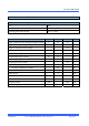
J1 Pin Configuration
Signal Pin Description
C2CK 1 Clock signal for the C2 Debug Interface.
C2D 2 Bi-directional data signal for the C2 Debug Interface.
VCC 3 3.3 Volt power for the ZB-UPS01
TX 4 GPIO, also used as UART TX.
GND 5 Ground
RX 6 GPIO, also used as UART RX.
GPIO1 7 Bidirectional input/output Pin. It also can be programmed as analog to
digital converter (ADC1)
GPIO2 8 Bidirectional input/output Pin. It also can be programmed as analog to
digital converter (ADC2)
J2 Pin Configuration
Signal Pin Description
GPIO3 1 Bidirectional input/output Pin. It also can be programmed as analog to
digital converter (ADC3)
GPIO4 2 Bidirectional input/output Pin. It also can be programmed as analog to
digital converter (ADC4)
GPIO5 3 Bidirectional input/output Pin.
GPIO6 4 Bidirectional input/output Pin. It also can be programmed as analog to
digital converter (ADC5)
GPIO7 5 Bidirectional input/output Pin. It also can be programmed as analog to
digital converter (ADC6)
GPIO8 6 Bidirectional input/output Pin.