
Owner manual


Table Of Contents
- NANO-LX EPIC SBC User Manual
- 1 Introduction
- 2 Detailed Specifications
- 2.1 Overview
- 2.2 Dimensions
- 2.3 Data Flow
- 2.4 CPU Support
- 2.5 System Chipset
- 2.5.1 GeodeLink™ Interface Unit
- 2.5.2 AMD® Geode™ CS5536 ATA-6 Controller
- 2.5.3 AMD® Geode™ CS5536 Audio Codec 97 (AC’97) Controller
- 2.5.4 AMD® Geode™ CS5536 Flash Interface
- 2.5.5 AMD® Geode™ CS5536 USB Controller
- 2.5.6 AMD® Geode™ CS5536 Serial Communications
- 2.5.7 AMD® Geode™ CS5536 Real Time Clock
- 2.5.8 BIOS
- 2.6 GeodeLink™ PCI Bridge
- 2.7 Environmental and Power Specifications
- 3 Unpacking
- 4 Connectors and Jumpers
- 4.1 Peripheral Interface Connectors
- 4.2 Internal Peripheral Connectors
- 4.2.1 ATX Connector
- 4.2.2 ATX Power Button
- 4.2.3 Audio CD-In Connector
- 4.2.4 Audio Connector
- 4.2.5 Battery Connector
- 4.2.6 Compact Flash Connector
- 4.2.7 Digital Input Output Connector
- 4.2.8 Fan Connector
- 4.2.9 FDD Connector
- 4.2.10 IDE Interface Connector
- 4.2.11 Inverter Connector
- 4.2.12 IrDA Connector
- 4.2.13 Keyboard/Mouse Connector
- 4.2.14 LED Power Connector
- 4.2.15 LVDS LCD Panel Connector
- 4.2.16 Parallel Port Connector
- 4.2.17 PC/104-Plus Connector
- 4.2.18 Power Connector
- 4.2.19 Power Input Connector
- 4.2.20 Reset Button Connector
- 4.2.21 SATA Drive Ports
- 4.2.22 Serial Communications Connector
- 4.2.23 TFT TTL LCD Connector
- 4.3 External (Rear Panel) Connectors
- 5 Installation and Configuration
- 6 Award BIOS Setup
- 7 Software Drivers
- A BIOS Configuration Options
- B Watchdog Timer
- C Address Mapping
- D External AC’97 Audio CODEC
- E ALi® RAID for SATA
- F Connecting an ATX Power Supply
- G Index
NANO-LX EPIC SBC
Pin Row A Row B Row C Row D
30 SA1 OSC -- --
31 SA0 GND -- --
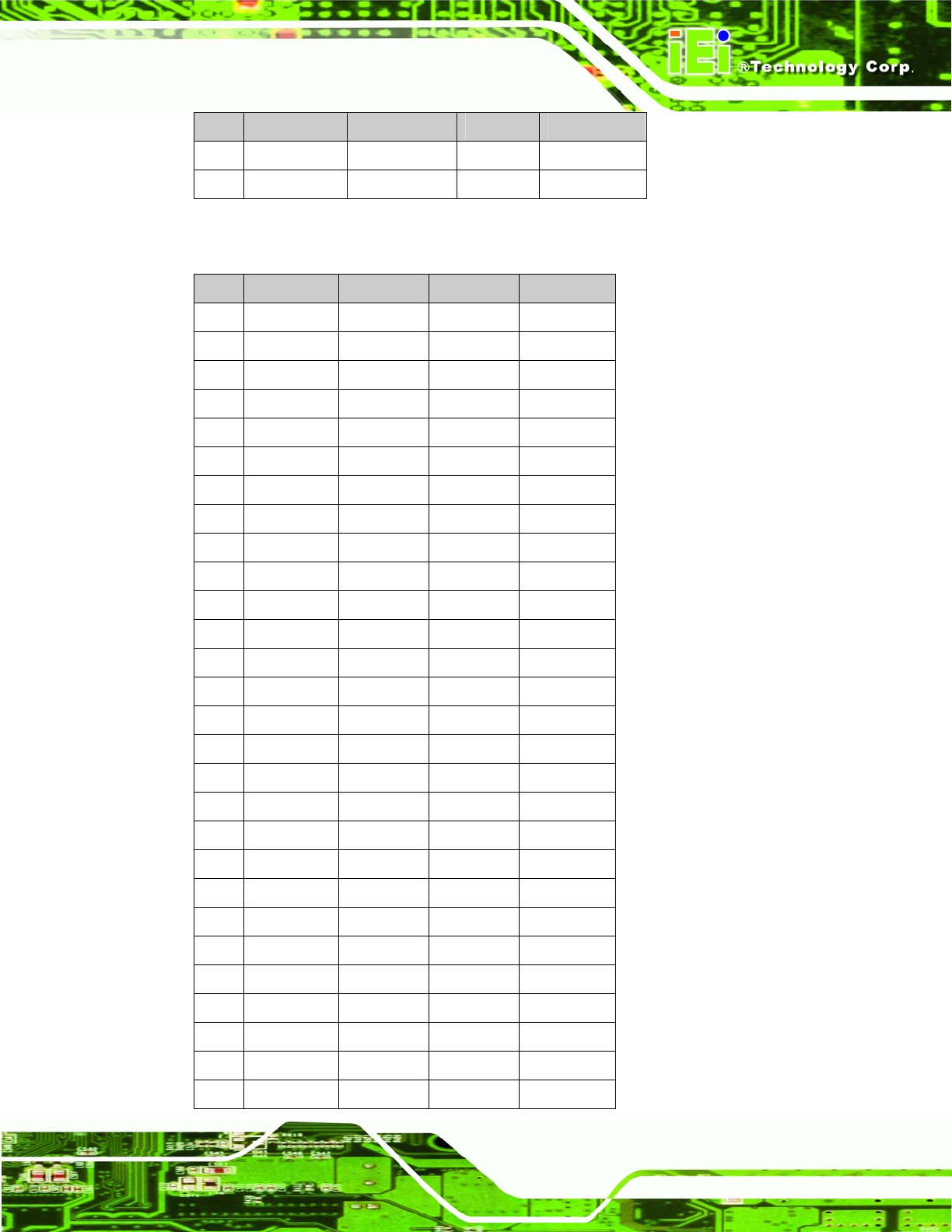
Table 4-20: CN7 (PC/104) Connector Pinouts
Pin A B C D
1 GROUND TBD1 +5V AD0
2 VIO AD2 AD1 +5V
3 AD5 GND AD4 AD3
4 CBE0- AD7 GND AD6
5 GND AD9 AD8 GND
6 AD11 VIO AD10 N66EV
7 AD14 AD13 GND AD12
8 +3.3V CBE1- AD15 +3.3V
9 SERR- GND SBO- PAR
10 GND PERR- +3.3V SDONE
11 STOP- +3.3V LOCK- GND
12 +3.3V TRDY- GND DEVSEL-
13 FRAME- GND IRDY- +3.3V
14 GND AD16 +3.3V CBE2-
15 AD18 +3.3V AD17 GND
16 AD21 AD20 GND AD19
17 +3.3V AD23 AD22 +3.3V
18 IDSEL0 GND IDSEL1- IDSEL2
19 AD24 CBE3- VIO IDSEL3
20 GND AD26 AD25 GND
21 AD29 +5V AD28 AD27
22 +5V AD30 GND AD31
23 REQ0- GND REQ1- VIO
24 GND REQ2- +5V GNT0-
25 GNT1- VIO GNT2- GND
26 +5V PCICLK0 GND PCICLK1
27 PCICLK2 +5V PCICLK3 GND
28 GND INTD- +5V PCIRST-
Page 71