
Manual


PCISA -9652 Half-Size CPU Card
Page 49
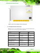
CN Location: See Figure 4-7
CN Pinouts: See
Table 4-7
The DIO connector is managed through a Super I/O chip. The DIO connector pins are
user programmable. The digital IO port of PCISA-9652 is 5V CMOS level.
Figure 4-7: GPIO Connector Location
PIN NO. DESCRIPTION PIN NO. DESCRIPTION
1 GND 2 VCC
3 OUTPUT 3 4 OUTPUT 2
5 OUTPUT 1 6 OUTPUT 0
7 INPUT 3 8 INPUT 2
9 INPUT 1 10 INPUT 0
Table 4-7: GPIO Connector Pinouts
4.2.6 Fan Connectors
CN Label: CPU_FAN1
CN Type:
4-pin wafer connector (1x3)
CN Location: See
Figure 4-8