
Manual


Table Of Contents
- 1 Introduction
- 2 Detailed Specifications
- 2.1 Dimensions
- 2.2 Data Flow
- 2.3 Embedded WAFER-945GSE Processor
- 2.4 Intel 945GSE Northbridge Chipset
- 2.5 Intel® ICH7-M Southbridge Chipset
- 2.6 LPC Bus Components
- 2.7 Environmental and Power Specifications
- 3 Unpacking
- 4 Connectors
- 4.1 Peripheral Interface Connectors
- 4.2 Peripheral Interface Connectors
- 4.3 Internal Peripheral Connectors
- 4.3.1 ATX Power Connector
- 4.3.2 ATX Power Supply Enable Connector
- 4.3.3 Audio Connector (10-pin)
- 4.3.4 Backlight Inverter Connector
- 4.3.5 CompactFlash® Socket
- 4.3.6 Digital Input/Output (DIO) Connector
- 4.3.7 Fan Connector (+12V, 3-pin)
- 4.3.8 Keyboard/Mouse Connector
- 4.3.9 LED Connector
- 4.3.10 LVDS LCD Connector
- 4.3.11 PCIe Mini Card Slot
- 4.3.12 Power Button Connector
- 4.3.13 Reset Button Connector
- 4.3.14 SATA Drive Connectors
- 4.3.15 Serial Port Connector (COM3, COM4, COM5 and COM6)
- 4.3.16 Serial Port Connector (COM 2)(RS-232, RS-422 or RS-485)
- 4.3.17 USB Connectors (Internal)
- 4.4 External Peripheral Interface Connector Panel
- 5 Installation
- 5.1 Anti-static Precautions
- 5.2 Installation Considerations
- 5.3 Unpacking
- 5.4 SO-DIMM and CF Card Installation
- 5.5 Jumper Settings
- 5.6 Chassis Installation
- 5.7 Internal Peripheral Device Connections
- 5.7.1 Peripheral Device Cables
- 5.7.2 SATA Drive Connection
- 5.7.3 Serial Port Connector Cable (Four Ports) Cable Connection
- 5.7.4 Dual RS-232 Cable Connection (w/o bracket) (Optional)
- 5.7.5 4-COM Port Adapter Board Connection (Optional)
- 5.7.6 Keyboard/Mouse Y-cable Connector
- 5.7.7 Audio Kit Installation
- 5.7.8 USB Cable (Dual Port without Bracket) (Optional)
- 5.8 External Peripheral Interface Connection
- 5.9 Heat Sink Enclosure
- 6 BIOS Screens
- 7 Software Drivers
- A BIOS Menu Options
- B Terminology
- C DIO Interface
- D Watchdog Timer
- E Address Mapping
- F Hazardous Materials Disclosure
WAFER-945GSE 3.5” Motherboard
Page 170
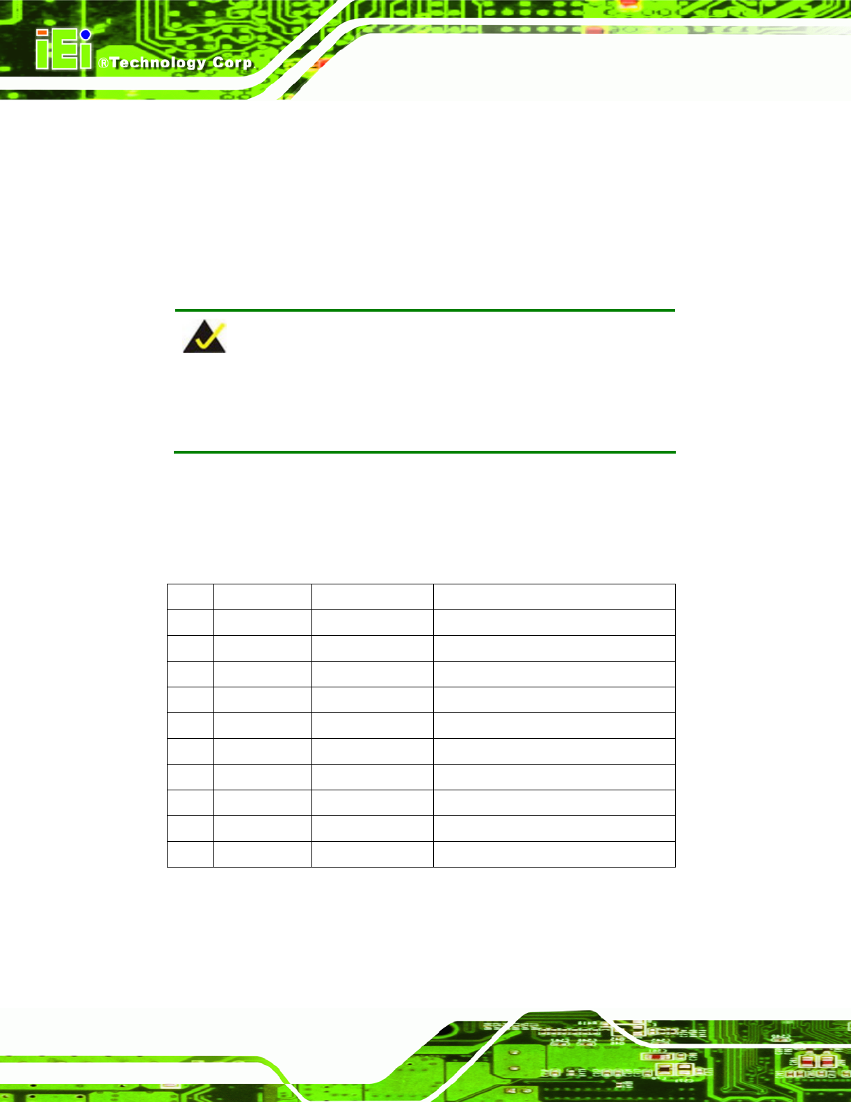
C.1 DIO Interface Introduction
The DIO connector on the WAFER-945GSE is interfaced to GPIO ports on the ITE
IT8718F Super I/O chipset. The DIO has both 4-bit digital inputs and 4-bit digital outputs.
The digital inputs and digital outputs are generally control signals that control the on/off
circuit of external devices or TTL devices. Data can be read or written to the selected
address to enable the DIO functions.
NOTE:
For further information, please refer to the datasheet for the ITE
IT8718F Super I/O chipset.
C.2 DIO Connector Pinouts
The following table describes how the DIO connector pins are connected to the Super I/O
GPIO port.
Pin Description Super I/O Pin Super I/O Pin Description
1 Ground N/A N/A
2 VCC N/A N/A
3 Output 3 GP23 General Purpose I/O Port 2 Bit 3
4 Output 2 GP22 General Purpose I/O Port 2 Bit 2
5 Output 1 GP21 General Purpose I/O Port 2 Bit 1
6 Output 0 GP20 General Purpose I/O Port 2 Bit 0
7 Input 3 GP33 General Purpose I/O 33
8 Input 2 GP32 General Purpose I/O 32
9 Input 1 GP31 General Purpose I/O 31
10 Input 0 GP30 General Purpose I/O 30