
Manual


Table Of Contents
- 1 Introduction
- 2 Detailed Specifications
- 2.1 Dimensions
- 2.2 Data Flow
- 2.3 Embedded WAFER-945GSE Processor
- 2.4 Intel 945GSE Northbridge Chipset
- 2.5 Intel® ICH7-M Southbridge Chipset
- 2.6 LPC Bus Components
- 2.7 Environmental and Power Specifications
- 3 Unpacking
- 4 Connectors
- 4.1 Peripheral Interface Connectors
- 4.2 Peripheral Interface Connectors
- 4.3 Internal Peripheral Connectors
- 4.3.1 ATX Power Connector
- 4.3.2 ATX Power Supply Enable Connector
- 4.3.3 Audio Connector (10-pin)
- 4.3.4 Backlight Inverter Connector
- 4.3.5 CompactFlash® Socket
- 4.3.6 Digital Input/Output (DIO) Connector
- 4.3.7 Fan Connector (+12V, 3-pin)
- 4.3.8 Keyboard/Mouse Connector
- 4.3.9 LED Connector
- 4.3.10 LVDS LCD Connector
- 4.3.11 PCIe Mini Card Slot
- 4.3.12 Power Button Connector
- 4.3.13 Reset Button Connector
- 4.3.14 SATA Drive Connectors
- 4.3.15 Serial Port Connector (COM3, COM4, COM5 and COM6)
- 4.3.16 Serial Port Connector (COM 2)(RS-232, RS-422 or RS-485)
- 4.3.17 USB Connectors (Internal)
- 4.4 External Peripheral Interface Connector Panel
- 5 Installation
- 5.1 Anti-static Precautions
- 5.2 Installation Considerations
- 5.3 Unpacking
- 5.4 SO-DIMM and CF Card Installation
- 5.5 Jumper Settings
- 5.6 Chassis Installation
- 5.7 Internal Peripheral Device Connections
- 5.7.1 Peripheral Device Cables
- 5.7.2 SATA Drive Connection
- 5.7.3 Serial Port Connector Cable (Four Ports) Cable Connection
- 5.7.4 Dual RS-232 Cable Connection (w/o bracket) (Optional)
- 5.7.5 4-COM Port Adapter Board Connection (Optional)
- 5.7.6 Keyboard/Mouse Y-cable Connector
- 5.7.7 Audio Kit Installation
- 5.7.8 USB Cable (Dual Port without Bracket) (Optional)
- 5.8 External Peripheral Interface Connection
- 5.9 Heat Sink Enclosure
- 6 BIOS Screens
- 7 Software Drivers
- A BIOS Menu Options
- B Terminology
- C DIO Interface
- D Watchdog Timer
- E Address Mapping
- F Hazardous Materials Disclosure
WAFER-945GSE 3.5” Motherboard
Page 54
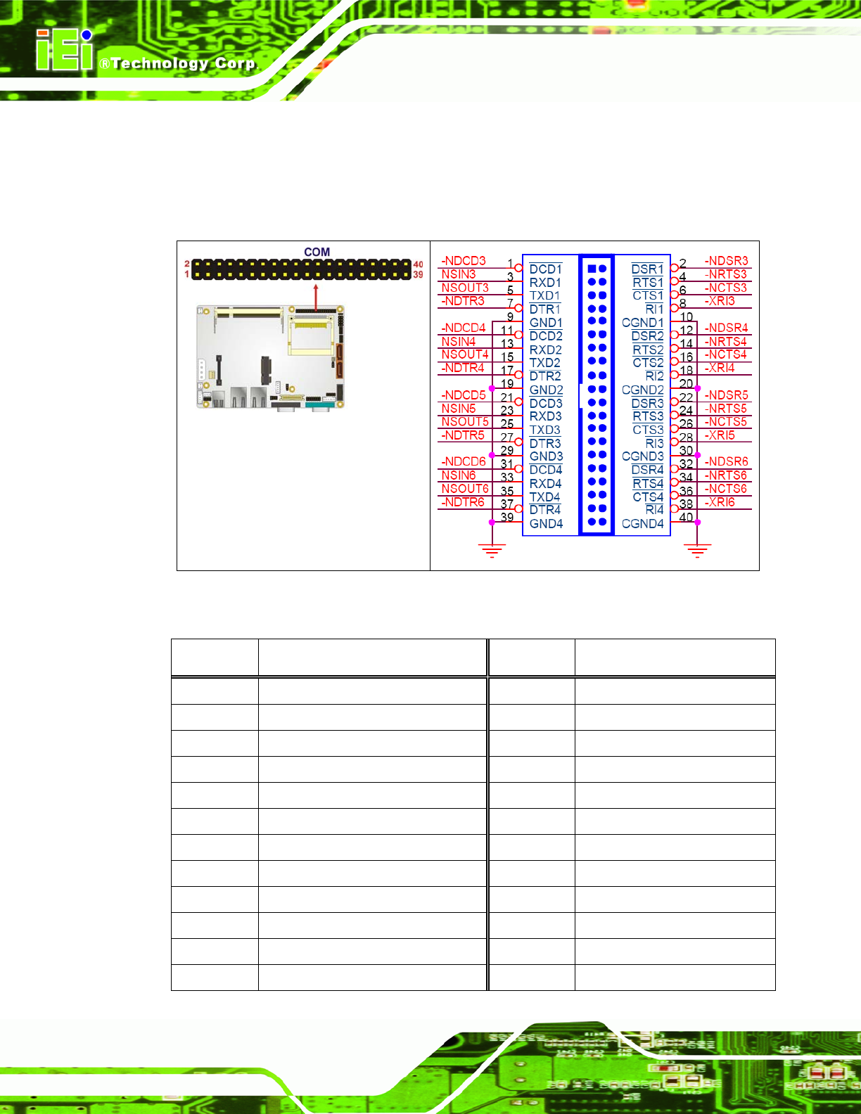
COM3 is located on pin 1 to pin 10
COM4 is located on pin 11 to pin 20
COM5 is located on pin 21 to pin 30
COM6 is located on pin 31 to pin 40
Figure 4-16: COM3 to COM6 Connector Pinout Locations
PIN NO. DESCRIPTION PIN NO. DESCRIPTION
1 DATA CARRIER DETECT (DCD3)
2 DATA SET READY (DSR3)
3 RECEIVE DATA (RXD3) 4 REQUEST TO SEND (RTS3)
5 TRANSMIT DATA (TXD3) 6 CLEAR TO SEND (CTS3)
7 DATA TERMINAL READY (DTR3)
8 RING INDICATOR (RI3)
9 GND 10 GND
11 DATA CARRIER DETECT (DCD4)
12 DATA SET READY (DSR4)
13 RECEIVE DATA (RXD4) 14 REQUEST TO SEND (RTS4)
15 TRANSMIT DATA (TXD4) 16 CLEAR TO SEND (CTS4)
17 DATA TERMINAL READY (DTR4)
18 RING INDICATOR (RI4)
19 GND 20 GND
21 DATA CARRIER DETECT (DCD5)
22 DATA SET READY (DSR5)
23 RECEIVE DATA (RXD5) 24 REQUEST TO SEND (RTS5)