
Manual
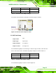
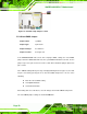


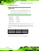
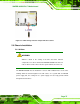


Table Of Contents
- 1 Introduction
- 2 Detailed Specifications
- 2.1 Dimensions
- 2.2 Data Flow
- 2.3 Embedded WAFER-945GSE Processor
- 2.4 Intel 945GSE Northbridge Chipset
- 2.5 Intel® ICH7-M Southbridge Chipset
- 2.6 LPC Bus Components
- 2.7 Environmental and Power Specifications
- 3 Unpacking
- 4 Connectors
- 4.1 Peripheral Interface Connectors
- 4.2 Peripheral Interface Connectors
- 4.3 Internal Peripheral Connectors
- 4.3.1 ATX Power Connector
- 4.3.2 ATX Power Supply Enable Connector
- 4.3.3 Audio Connector (10-pin)
- 4.3.4 Backlight Inverter Connector
- 4.3.5 CompactFlash® Socket
- 4.3.6 Digital Input/Output (DIO) Connector
- 4.3.7 Fan Connector (+12V, 3-pin)
- 4.3.8 Keyboard/Mouse Connector
- 4.3.9 LED Connector
- 4.3.10 LVDS LCD Connector
- 4.3.11 PCIe Mini Card Slot
- 4.3.12 Power Button Connector
- 4.3.13 Reset Button Connector
- 4.3.14 SATA Drive Connectors
- 4.3.15 Serial Port Connector (COM3, COM4, COM5 and COM6)
- 4.3.16 Serial Port Connector (COM 2)(RS-232, RS-422 or RS-485)
- 4.3.17 USB Connectors (Internal)
- 4.4 External Peripheral Interface Connector Panel
- 5 Installation
- 5.1 Anti-static Precautions
- 5.2 Installation Considerations
- 5.3 Unpacking
- 5.4 SO-DIMM and CF Card Installation
- 5.5 Jumper Settings
- 5.6 Chassis Installation
- 5.7 Internal Peripheral Device Connections
- 5.7.1 Peripheral Device Cables
- 5.7.2 SATA Drive Connection
- 5.7.3 Serial Port Connector Cable (Four Ports) Cable Connection
- 5.7.4 Dual RS-232 Cable Connection (w/o bracket) (Optional)
- 5.7.5 4-COM Port Adapter Board Connection (Optional)
- 5.7.6 Keyboard/Mouse Y-cable Connector
- 5.7.7 Audio Kit Installation
- 5.7.8 USB Cable (Dual Port without Bracket) (Optional)
- 5.8 External Peripheral Interface Connection
- 5.9 Heat Sink Enclosure
- 6 BIOS Screens
- 7 Software Drivers
- A BIOS Menu Options
- B Terminology
- C DIO Interface
- D Watchdog Timer
- E Address Mapping
- F Hazardous Materials Disclosure
WAFER-945GSE 3.5” Motherboard
Page 72
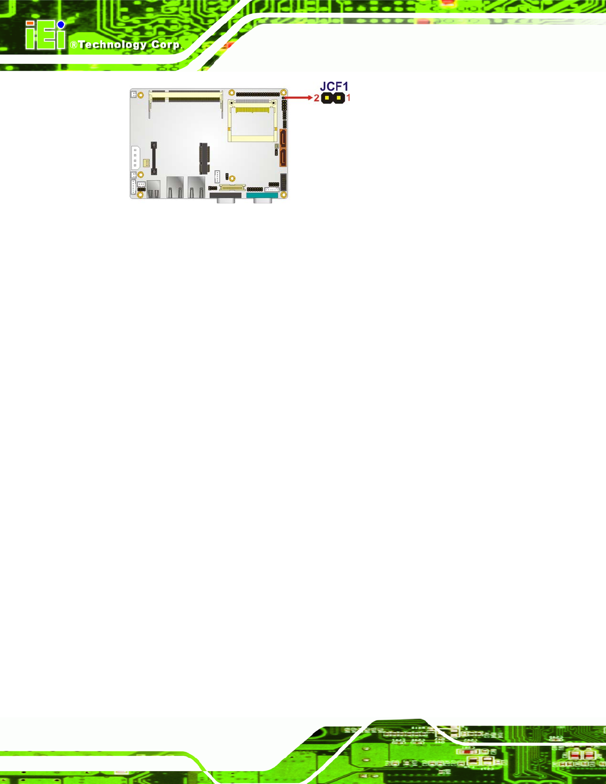
Figure 5-5: CF Card Setup Jumper Location
5.5.3 Clear CMOS Jumper
Jumper Label:
J_CMOS1
Jumper Type:
3-pin header
Jumper Settings:
See
830H790HTable 5-4
Jumper Location:
See
831H791HFigure 5-6
If the WAFER-945GSE fails to boot due to improper BIOS settings, the clear CMOS
jumper clears the CMOS data and resets the system BIOS information. To do this, use the
jumper cap to close pins 2 and 3 for a few seconds then reinstall the jumper clip back to
pins 1 and 2.
If the “CMOS Settings Wrong” message is displayed during the boot up process, the fault
may be corrected by pressing the F1 to enter the CMOS Setup menu. Do one of the
following:
Enter the correct CMOS setting
Load Optimal Defaults
Load Failsafe Defaults.
After having done one of the above, save the changes and exit the CMOS Setup menu.
The clear CMOS jumper settings are shown in
832H792HTable 5-4.